Introduction
Wide-bandgap (WBG) devices have revolutionized modern power electronics. Owing to higher efficiency, switching speed, power density, and improved thermal management, GaN transistors (GaN) and Silicon Carbide (SiC) MOSFETs are increasingly replacing traditional Si power semiconductors in multiple applications.
WBG devices offer several advantages over Si power semiconductors, but these devices are not interchangeable in all applications. Each device has its own strengths and limitations; hence it is critical to understand which device should be used in a specific application.
Selection of appropriate WBG semiconductor depends on application type, voltage requirements, thermal limits, switching frequency, and efficiency targets.
This guide compares SiC and GaN devices in terms of switching behaviour, thermal performance, losses, and cost, helping engineers to choose a specific device for their application.
Traditional vs Modern Power Semiconductors (Si vs SiC and GaN)
Traditional Si devices face several limitations in many applications. The table below highlights limitations of Si devices and how WBG devices are used to overcome those limitations.
| Limitations of Si devices | How WBG devices help |
| Higher switching losses at high frequency | Lower switching losses enable higher efficiency |
| Limited temperature capability | Operate at higher junction temperatures |
| Higher conduction losses at high voltage | Lower conduction losses, especially in high-voltage applications |
| Lower power density | Higher power density allows smaller designs |
| Limited high-frequency performance | Support much higher switching frequencies |
| Larger passive components required | Smaller inductors and capacitors due to high frequency |
| Reduced efficiency in demanding applications | Improved overall system efficiency |
What is SiC MOSFET?
A SiC MOSFET is high-frequency power semiconductor devices made from a compound of silicon and carbide. This device is specifically designed for high power high frequency applications. The table below presents key strengths and applications of SiC MOSFETs.
| Key strengths | Applications |
| High voltage capability | EV traction inverters |
| Lower switching losses | Solar inverters |
| Excellent thermal properties | Industrial supplies |
| Highly suitable in harsh environments | Motor drives |
| High ruggedness | High voltage DC-DC converters |
What is GaN Transistor
Gallium Nitride (GaN) devices are high performance power semiconductors made from GaN. These devices are faster, smaller and more efficient compared to conventional Si power semiconductors (For example: GNP2070TD-ZTR). The table below presents key strengths and applications of GaN transistors.
| Key strengths | Applications |
| Extremely fast switching | Fast chargers |
| Low gate charge | Power supplies |
| Lower output capacitance | RF systems |
| Reduced switching losses | DC-DC converters |
| Higher power density | Power adapters |
GaN vs SiC: Key Differences and Performance Comparison
Device performance is strongly influenced by material properties. This section compares the performance of GaN and SiC devices in terms of switching behavior, conduction losses, thermal performance, voltage capability, and efficiency.
Switching Behaviour in GaN vs SiC Devices
Switching losses in power semiconductors are approximated as:
\[P_{sw}=\frac{1}{2}VI(t_r+t_f)f_s\]
Where:
V= switching voltage
I= current
tr= rise time
tf= fall time
fs= switching frequency
From the given equation, switching losses are directly proportional to switching time, which means device with faster switching transitions leads to lower switching losses.
While comparing with SiC, GaN devices often have lower tr and tf that enables smaller passive components and higher power density. This means GaN devices are more suitable for high frequency applications.
Conduction losses
Conduction losses normally occur when the device is conducting. Mathematically, they are given as:
\[P_{cond}=I^2R_{DS(on)}\]
From the equation above, conduction losses are proportional to Rds(on) that means device with higher Rds(on) will lead to higher conduction losses (assuming same current in both devices).
SiC devices maintain stable Rds(on) across a wide temperature range making them highly suitable for high-power applications. In contrast, GaN devices exhibit lower Rds(on) at lower voltage rating. Their structure allows for efficient current conduction with minimal resistance, especially in high-frequency applications (See Fig-1).

Note: Curves are illustrative and represent general trends. Actual behavior depends on specific devices and datasheets.
Voltage Capability
Voltage capability is one of the important factors in device selection. GaN devices are rated up to 650V(such as Nexperia GAN041-650WSBQ), hence these devices are suitable for low-medium power applications.
In contrast, the breakdown voltage for SiC devices are much higher and can reach up to 1.2kV. These devices are efficient in high-power applications.
Thermal Performance
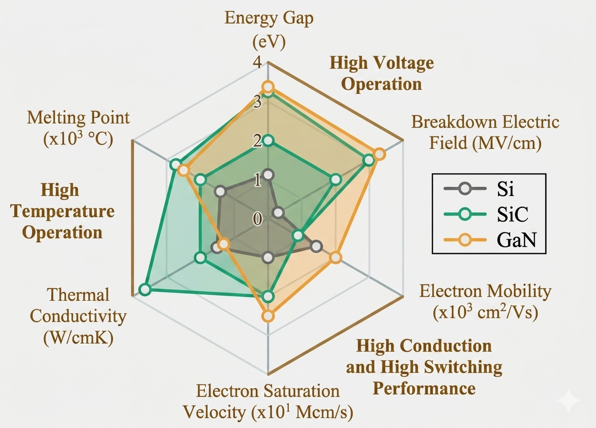
SiC power semiconductors are often superior to GaN devices in terms of thermal performance. SiC has thermal conductivity roughly three times higher than GaN devices, making them suitable for high-temperature applications such as automotive, industrial and high-density power systems.
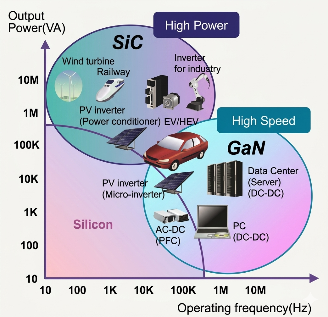
Switching Frequency and Power density
Switching frequency directly affects the size of the system as higher frequency leads to lower passive components. Comparing with SiC devices, GaN can work at much higher frequency while maintaining the lower switching losses.
Hence, GaN enables compact and lightweight designs, especially in chargers and server power supplies (See Fig-2).
GaN vs SiC: PCB Layout Considerations
PCB layout is extremely important when working with WBG devices. GaN devices being very fast leads to high di/dt and dv/dt issues. This increases ringing, EMI challenges and layout sensitivity. This demands an extra care in GaN PCB layout compared to SiC to avoid excessive heat generation and device failure due to board parasitics.
GaN vs SiC: Internal Inductance
Internal inductance is one of the important parameters during the choice of GaN and SiC devices. SiC devices often come in TO-247 or D2PAK while GaN devices are typically surface mounted devices (SMD). Hence, GaN devices has lower internal inductance compared to SiC MOSFETs.
\[V_{peak}=L\times \frac{di}{dt}\]
A di/dt of 100A/ns is common which means even 1nH of lead inductance can create a 100V spike. This is why GaN requires tight PCB layouts to avoid device failure.
Gate Drive Requirements
Gate driver design for SiC and GaN differs substantially. SiC devices typically requires +15V to +20V to turn on, while GaN device has lower gate voltage requirements and requires precise gate control (such as Navitas NV6125).
For turn off, negative voltage is used in GaN devices, whereas SiC devices are generally driven to 0 V or a small negative voltage to prevent unintended turn-on.
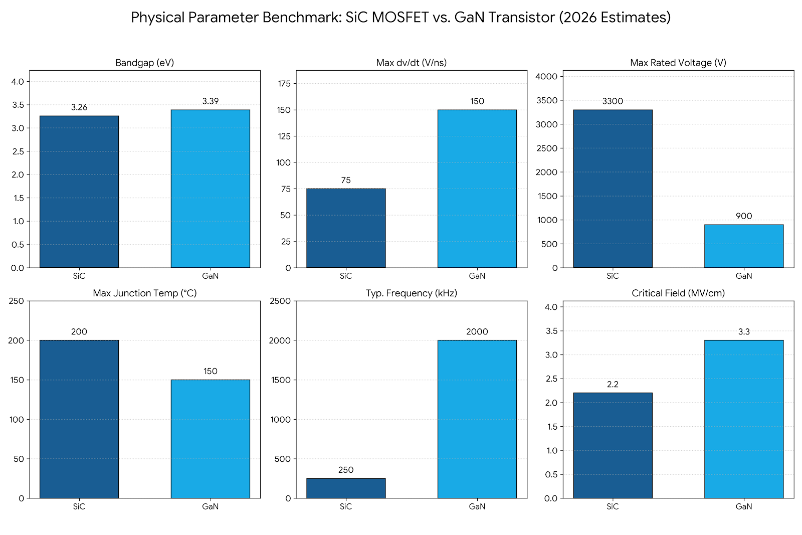
In addition, Table below shows a quick comparison of different parameters of GaN and SiC power semiconductors (Also see Fig-3 and Fig-4).
| Parameter | GaN Transistor | SiC MOSFET |
| Bandgap | Wider | Wide |
| Switching speed | Very high | High |
| Voltage capability | Moderate to high | Excellent |
| Temperature capability | Good | Excellent |
| Frequency capability | Very high | High |
| Ruggedness | Moderate | Very Strong |
| Power Density | Very high | High |
Case Study 1: Designing 22kW On-Board Charger (OBC)
Problem
An automotive OEM needs to design 22kW On-Board Charger (OBC) that should fit within the same physical footprint as their previous 11kW design with Si based power semiconductor.
Solution
This needs a significant improvement in power density while maintaining high efficiency and thermal performance. In this case, designers decided to use 800V architecture to improve efficiency and reduce current levels.
Although GaN devices are technically capable for this power level, however due to their lateral heat dissipation characteristics, thermal management will be significant challenge.
Hence, designers choose SiC MOSFET (TO-247 Package) with kelvin source pin. This additional pin plays an essential role in separating power loop from gate drive loop, thus minimizing di/dt issues.
\[V_{G_{internal}} = V_{G_{applied}} – \left(L_s \times \frac{di}{dt}\right)\]
This configuration helps in reducing the ringing and improving switch reliability [How to Choose the Right Capacitor for Power Supply Design]. To summarize, SiC is the preferred choice for high-power, high-voltage automotive systems where efficiency, thermal performance, and robustness are critical.
Case Study 2: 240 W USB-C Fast Charger
Problem
A 240W USB-C fast charger needs to be designed. The charger must operate at higher switching frequency to reduce size of passive components and achieve low form factor.
Solution
When designing a fast charger, maintaining high power density while ensuring efficient operation is a key objective.
In this scenario, GaN devices (IGT65R035D2ATMA1) are the preferred choice due to their fast-switching capability. These devices are capable of working at very high switching frequencies, allowing designers to reduce the size of magnetics and other passive components.
Additionally, GaN devices offer lower switching losses, which helps improve efficiency and supports high power density requirements.
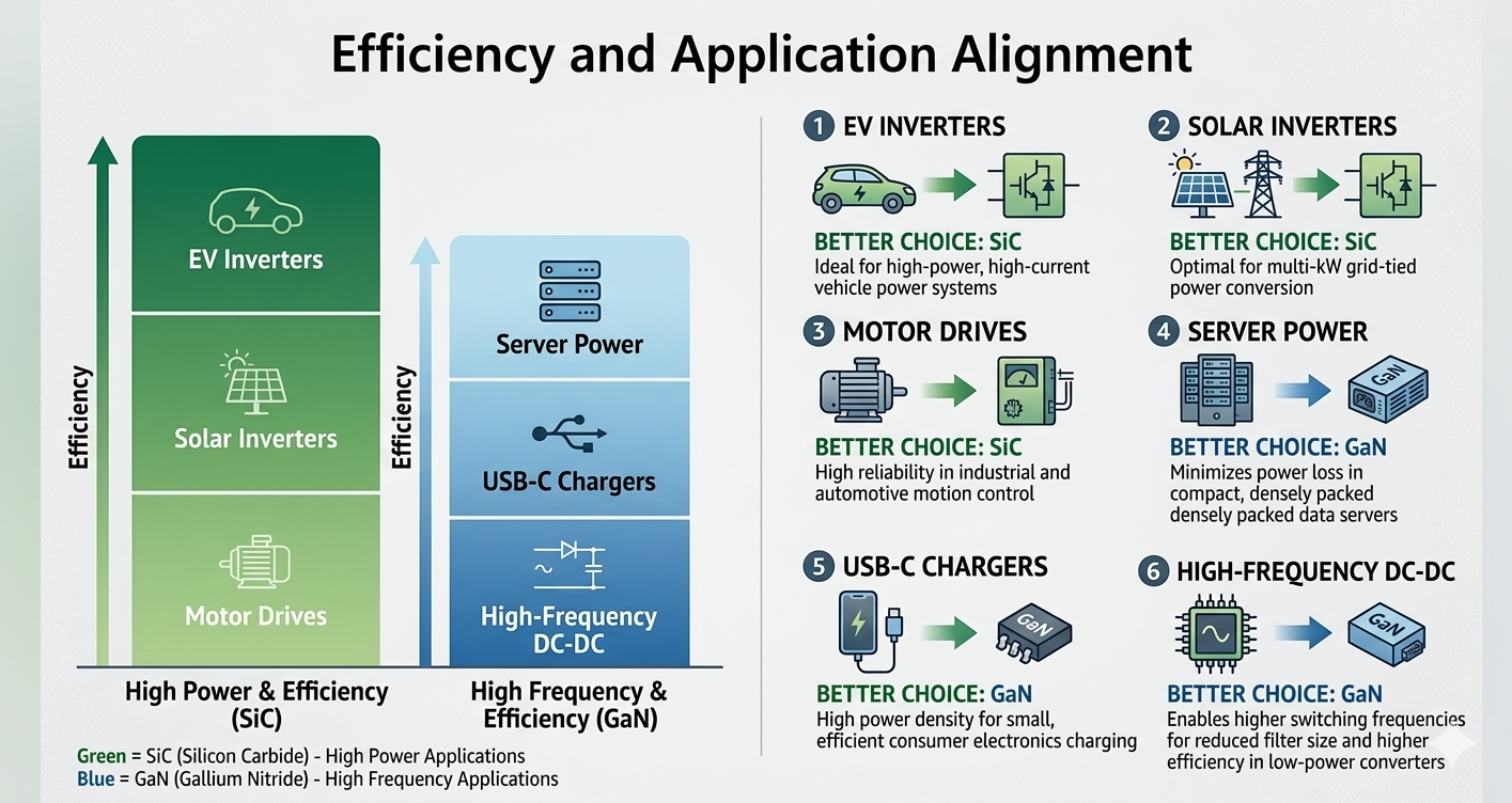
GaN vs SiC: Efficiency Comparison by Application
It is worth noting that there is no universal winner among power semiconductors. The choice of WBG device depends on several factors. The table below refers to the choice of WBG based on the specific application (See Fig-5).
| Application | Better Choice |
| EV Inverters | SiC |
| Solar Inverters | SiC |
| Motor Drives | SiC |
| Server Power | GaN |
| USB-C Chargers | GaN |
| High-Frequency DC-DC | GaN |
GaN vs SiC: Quick Selection Table
| If You Prioritize | Choose |
| High voltage | SiC |
| Thermal robustness | SiC |
| Ruggedness | SiC |
| Ultra-fast switching | GaN |
| Smallest size | GaN |
| Highest power density | GaN |
GaN vs SiC: Recent Trends in 2026
| SiC trends | GaN trends |
| Grid power conversion | High-density DC-DC converters |
| Energy storage | Fast charging |
| EV platforms | Data centre power supplies |
| High-power industrial systems | RF systems |
Common Mistakes When Selecting GaN or SiC
Although datasheets provide most of the information required to select suitable WBG device for specific applications. However, designers often make some common mistakes that can lead to poor performance. The common mistakes are:
- Ignoring system-level trade-offs
- Selecting based on cost only
- Overlooking gate driver requirements
- Not considering PCB layout issues
Conclusions
This article presents a comparison guide that helps in selecting a suitable WBG (GaN vs SiC) device for a specific application. There is no single winner in 2026, when comparing GaN transistor with SiC MOSFET.
SiC devices are preferred when high voltage and better thermal performance is required. In contrast, GaN dominates in high switching speed and power density applications such as compact high-frequency converters.
To conclude, appropriate choice of WBG device depends less on which device is better and more on what a specific application demands. The important parameters are breakdown voltage, switching frequency, thermal constraints, layout complexity and system-level performance.
Frequently Asked Questions (FAQs)
Typically, no. GaN devices are extremely sensitive and require maximum gate voltage of 6V-7V. However, a standard MOSFET driver supplies 12-15V which can destroy gate oxide. Hence, a dedicated GaN gate driver is preferred.
From the device point of view, SiC devices are more expensive than GaN devices. However, SiC devices can be cheaper at system-level, as they reduce cost and size of the heatsink in high-power applications.
Cascode GaN is a power semiconductor configuration combining a high-voltage, normally-on GaN HEMT with a low-voltage, normally-off Silicon MOSFET. This combination enables to use standard MOSFET driver while getting switching benefits of GaN transistor.
No. These devices offer different benefits and can be used in different applications. They are considered more complementary than direct replacements.
COMMENTS