What is the MAX232 IC?
The MAX232 is a dual RS-232 transceiver IC that converts TTL/CMOS logic-level signals (0–5 V) to RS-232 voltage levels (approximately ±7.5 V to ±10 V) and vice versa. It operates from a single +5 V power supply and uses an internal charge pump with four external capacitors to generate the positive and negative RS-232 voltages. As a result, no external ±12 V power supply is needed.
| Parameter | Value / Range |
|---|---|
| Supply Voltage | Single +5 V (VCC range: 4.5 V – 5.5 V) |
| Supply Current | 8 mA typical (no load) |
| Number of Drivers | 2 (TX channels) |
| Number of Receivers | 2 (RX channels) |
| RS-232 Output Voltage | ±7.5 V typical (meets TIA/EIA-232-F) |
| Receiver Input Range | Accepts ±30 V inputs |
| Receiver Threshold | 1.3 V typical, 0.5 V hysteresis |
| Max Data Rate | 120 kbps |
| Propagation Delay | < 10 µs |
| ESD Protection (HBM) | 2000 V (MAX232); 15 kV (MAX232E) |
| External Capacitors | 1.0 µF × 4 (original); 0.1 µF × 4 (MAX232A) |
| Package Options | PDIP-16, SOIC-16, SOP-16 |
| Operating Temperature | 0°C to +70°C (commercial) |
The Voltage Mismatch Problem
The UART interface on a microcontroller utilizes TTL/CMOS logic levels while an RS-232 serial port uses higher and inverted criteria for communicating between devices. This makes the two standards electrically incompatible; therefore, they cannot connect directly without using a level-shifting interface.
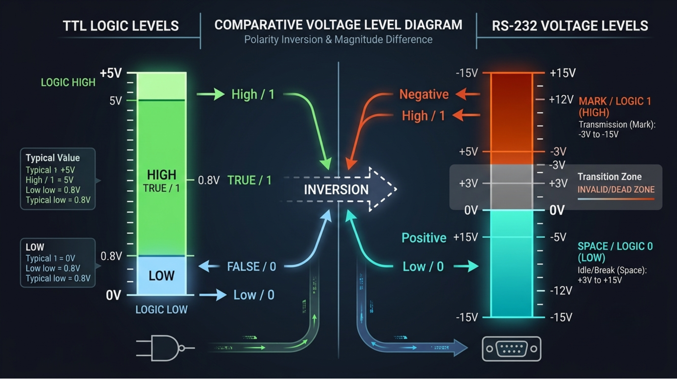
TTL logic defines logic low as 0 V and logic high as 5 V (or 3.3 V in newer systems). Most microcontrollers conform to this signalling method, including Arduino, PIC, AVR, and STM32 devices.
RS-232 is a standard that was created in 1962 by the Electronic Industries Association (EIA). The voltage levels used in an RS-232 connection are very different from what you may expect. It represents logic high (Mark) with a negative voltage (usually between -3 V and -15 V) and logic low (Space) with a positive voltage (usually between +3 V and +15 V).
A typical PC serial port uses voltage levels that can reach or exceed ±12 V. If someone connects these signals directly to a microcontroller GPIO or UART pin, they may exceed the device’s maximum voltage rating and cause permanent damage to the component.
Voltage-level conversion and signal inversion are necessary to establish a communication link between TTL and RS-232 devices. The MAX232 IC provides both functions in a single chip, so it enables communication between microcontrollers and RS-232 devices.
Maxim Integrated designed the MAX232 in the late 1980s. The industry quickly adopted it as the standard interface for microcontroller-to-PC serial communication. Texas Instruments currently manufactures it under the same part number, and several other manufacturers also produce compatible versions under different part numbers.
Understanding RS-232: The Standard Behind the Interface
RS-232 Voltage Levels and Logic Polarity
The TIA/EIA-232-F specification defines signal levels at the connectors, not at the IC pins of the equipment being used. The RS-232 drivers normally provide output signals with a voltage greater than ±5V. In contrast, the input signal values for RS-232 receivers have a range from a minimum of −3V up to at least +25V. However, RS-232 defines that the voltage levels between −3V and +3V fall into an undefined boundary, and therefore the system cannot rely upon these voltages to provide a reliable indication of a logic high or logic low.
The logic polarity of RS-232 and TTL logic is the reverse of one another. A logic high (Mark) in RS-232 is represented by a negative voltage, whereas a logic low (Space) is represented by a positive voltage. Interfaces between a microcontroller and an RS-232 device must therefore accommodate both voltage level conversions and signal inversions.
For example, when a microcontroller transmits a TTL logic 0 (LOW), the MAX232 typically outputs a positive RS-232 voltage. Likewise, the system converts a TTL logic 1 (HIGH) into a negative RS-232 voltage, ensuring compliance with the RS-232 standard.
The DB9 Connector and Signal Naming
Typically, RS-232 uses DE-9 connectors (also referred to as DB9 connectors) for device-to-device physical connections. While the RS-232 standard introduces several types of data and control signals, only a few are necessary for basic serial communications, including Pin 5 (GND) as the ground reference, Pin 3 (TD – Transmit Data) for sending data to an external device (i.e. microcontroller) from a PC, and Pin 2 (RD – Receive Data) to receive data from an external device to a PC. For those applications that require hardware flow control, two additional lines are also used: RTS (Request To Send) and CTS (Clear To Send).
It is essential to understand that the PC’s point of view defines RS-232 signal names. The PC transmits data through TD (Transmit Data), while the microcontroller receives the same data from that pin.Likewise, RD (Receive Data) on the PC side of the connection would be the TD on the microcontroller side, and vice versa. Understanding this difference between “Receive” and “Transmit” is essential for avoiding wiring errors, such as incorrect connections between terminals in both directions, and for ensuring the MAX232 interface circuit is configured correctly for proper signal direction and reliable communication.
MAX232 Electrical Specifications
The information was obtained from the Texas Instruments MAX232/MAX232I (Data Sheet SLLS047M – November 2014). Although Maxim Integrated produces a comparable version of this device, there are differences related to application circuits between the two manufacturers. For more information concerning these differences, refer to Section 5.
Single-Supply Operation
The MAX232 operates using a single +5 V supply, which eliminates the need for a −12 V source required in earlier RS-232 designs. Eliminating the −12V source results in a simpler circuit and a more efficient implementation in systems based upon microcontrollers. This was one of its main reasons for becoming popular in embedded applications. The MAX232, depending upon its operating state, will generally draw no more than 8 mA when idle.
Driver Output Voltage
MAX232 drivers convert TTL input signals into RS-232 voltage levels. Under typical operating conditions, the output voltage is approximately ±7.5 V. This meets the TIA/EIA-232-F standard, which requires a minimum output of ±5 V at the connector. The output voltage is slightly lower than the internal charge pump levels due to transistor voltage drops. However, it remains fully compliant and ensures reliable RS-232 communication.
Receiver Input Range and Threshold
The MAX232 receiver is intended to operate across a large input voltage range (between -30V and +30V). This will protect the device from accidental overvoltage conditions found on external RS-232 lines, and even if the actual input voltage is higher than the datasheet limits, the device will not be damaged. Typical switching thresholds for the MAX232 are approximately ±1.30V, which provides about ±0.50V of hysteresis. This allows for stable detection of signals without the need for additional noise filtering.
Data Rate
The MAX232 supports data rates of up to 120 kbps, making it suitable for standard serial communication applications. It works well with commonly used UART baud rates such as 9600, 19200, 38400, 57600, and 115200. This covers most embedded system communication requirements. However, for higher-speed applications above 230400 baud, improved versions like MAX232A are recommended. These variants offer better performance and signal integrity at higher speeds.
MAX232 Pinout: Every Pin Explained
The 16-pin package of the MAX232 chip allows for both prototyping and production designs. A common choice for prototyping using a breadboard is the DIP (dual in-line package) version because of its ease of handling and compatibility. The SOIC-16 package, on the other hand, is designed for surface-mount applications and is therefore useful in cramped PCB layouts.
While the package types differ physically, they both support the same electrical layout of pins, therefore providing the same functionality from one form factor to another.
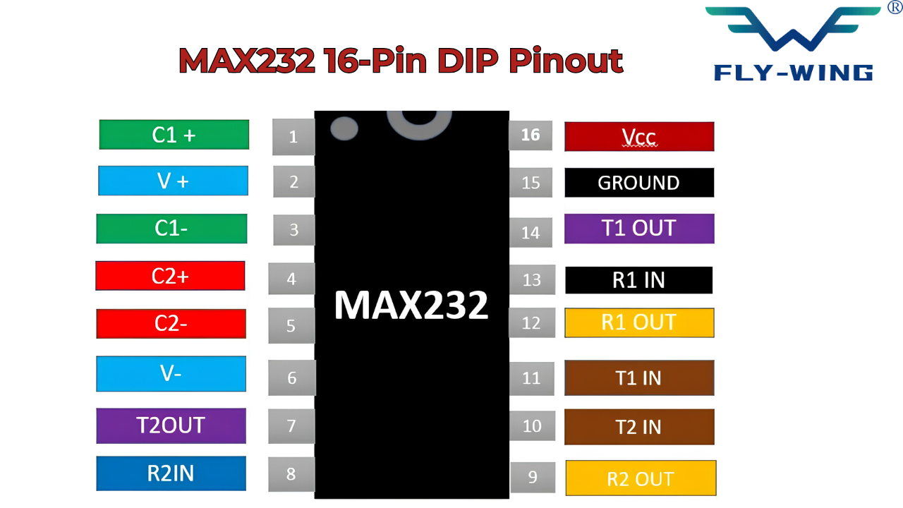
| Pin | Name | Function |
|---|---|---|
| 1 | C1+ | Positive terminal of charge pump flying capacitor C1 |
| 2 | V+ | Positive charge pump output (~+10 V); connect reservoir cap C3 to VCC |
| 3 | C1− | Negative terminal of charge pump flying capacitor C1 |
| 4 | C2+ | Positive terminal of charge pump flying capacitor C2 |
| 5 | C2− | Negative terminal of charge pump flying capacitor C2 |
| 6 | V− | Negative charge pump output (~−10 V); connect reservoir cap C4 to GND |
| 7 | T2OUT | RS-232 output of driver 2 — connect to RS-232 device RX line |
| 8 | R2IN | RS-232 input of receiver 2 — connect to RS-232 device TX line |
| 9 | R2OUT | TTL/CMOS output of receiver 2 — connect to MCU RX pin |
| 10 | T2IN | TTL/CMOS input of driver 2 — connect to MCU TX pin (channel 2) |
| 11 | T1IN | TTL/CMOS input of driver 1 — connect to MCU TX pin (primary channel) |
| 12 | R1OUT | TTL/CMOS output of receiver 1 — connect to MCU RX pin |
| 13 | R1IN | RS-232 input of receiver 1 — connect to DB9 pin 2 |
| 14 | T1OUT | RS-232 output of driver 1 — connect to DB9 pin 3 |
| 15 | GND | Ground — connect to system ground |
| 16 | VCC | Supply voltage +5 V — add 0.1 µF bypass capacitor to GND |
Understanding the Channel Layout
MAX232 IC features two sets of drivers and receivers, each set being equal to the other. Driver-receiver 1 works through pins 11 (T1IN), 14 (T1OUT), 13 (R1IN), and 12 (R1OUT), whereas driver-receiver 2 operates through pins 10 (T2IN), 7 (T2OUT), 8 (R2IN), and 9 (R2OUT). In most single-UART systems, driver-receiver 1 processes TX/RX signals, whereas driver-receiver 2 may process RTS and CTS signals.
T1IN stands for the TTL side of driver 1; T1OUT is the output of driver 1, RS-232 side; R1IN is the input of receiver 1, RS-232 side; and R1OUT is the output of receiver 1, TTL side. If you memorize such a definition, wiring mistakes will never occur.
How the MAX232 IC RS-232 TTL converter Charge Pump Works
It is the charge pump that makes the MAX232 IC RS-232 TTL converter special. The voltage levels of about +10V and -10V are obtained from a single 5V power source without using any transformer or separate power source. Only four capacitors and a switching oscillator do all this inside the IC.
Having understood it, everything else becomes clear. Capacitor placement and values will be very clear once the function of the capacitor is known.
Stage 1 — Voltage Doubler (Generating V+)
The initial stage of the charge pump circuit is called the voltage doubler. It operates through two phases. Phase 1 starts with the connection of the internal oscillator between capacitor C1 and the 5 V power source. C1 becomes charged to 5 V. Phase 2 involves disconnection of capacitor C1 from ground and connection to VCC. C1 is placed above the VCC power source. The positive plate of capacitor C1 reaches the level of 5 V due to the charging process, plus 5 V from VCC = 10 V. Reservoir capacitor C3 is charged to 10 V via a diode.
The oscillator switches all the time, and capacitor C3 is being replenished periodically. It leads to a steady +10 V power line formation in capacitor C3. This is the +V power source used by the RS-232 output driver to create positive RS-232 power lines.
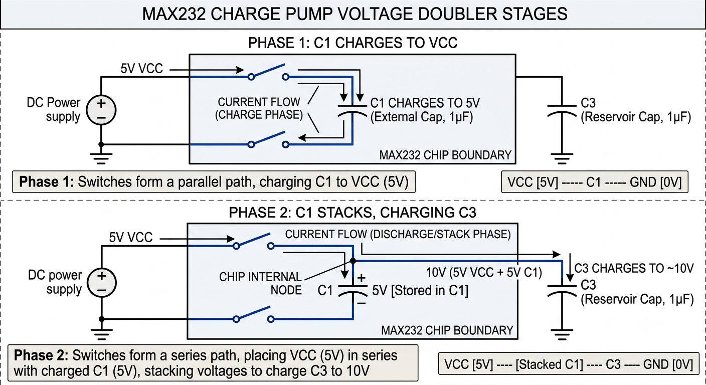
Stage 2 — Voltage Inverter (Generating V−)
The second stage of the charge pump circuit inverts the freshly generated voltage of +10 V. Phase one involves capacitor C2 charging with +10 V taken from the V+ line. Phase two sees the oscillator reversing the polarity of capacitor C2; that is, its positive leg connects with the ground potential, while the negative leg carries –10 V, which charges the reservoir capacitor C4. This yields the −10 V line on the capacitor C4, which serves as the V− power supply needed to create RS-232-compliant negative signals.
Thus, the full sequence looks like this: 5V power source → voltage doubler → +10V → inverter → −10V. The driver now possesses both power supplies needed to produce the required RS-232 voltage levels.
External Capacitor Requirements
The original MAX232 uses capacitors C1, C2, C3 and C4 of 1.0 µF. The frequency of the oscillator in an original MAX232 is relatively low and thus requires larger-sized capacitors to adequately store charge at that frequency. Either ceramic or tantalum capacitors may be used, but when using a tantalum capacitor, pay attention to the polarity; connecting a tantalum capacitor with the incorrect polarity could damage the capacitor as it is polarized.
Capacitors required by the MAX232A and MAX3232 are the same as those used with an original MAX232, except that they only require .01 µF capacitors. This is a much smaller, less expensive, and requires much less space on a PCB than the original. Therefore, they are the preferred choice for new designs.
Texas Instruments MAX232 variants may allow C3 to connect to either GND or VCC (as noted in the TI datasheet footnotes). However, because package markings do not always clearly identify the manufacturer, the safest and recommended practice is:
Always connect C3 to VCC (+5 V) — this is safe for both Maxim and TI versions.
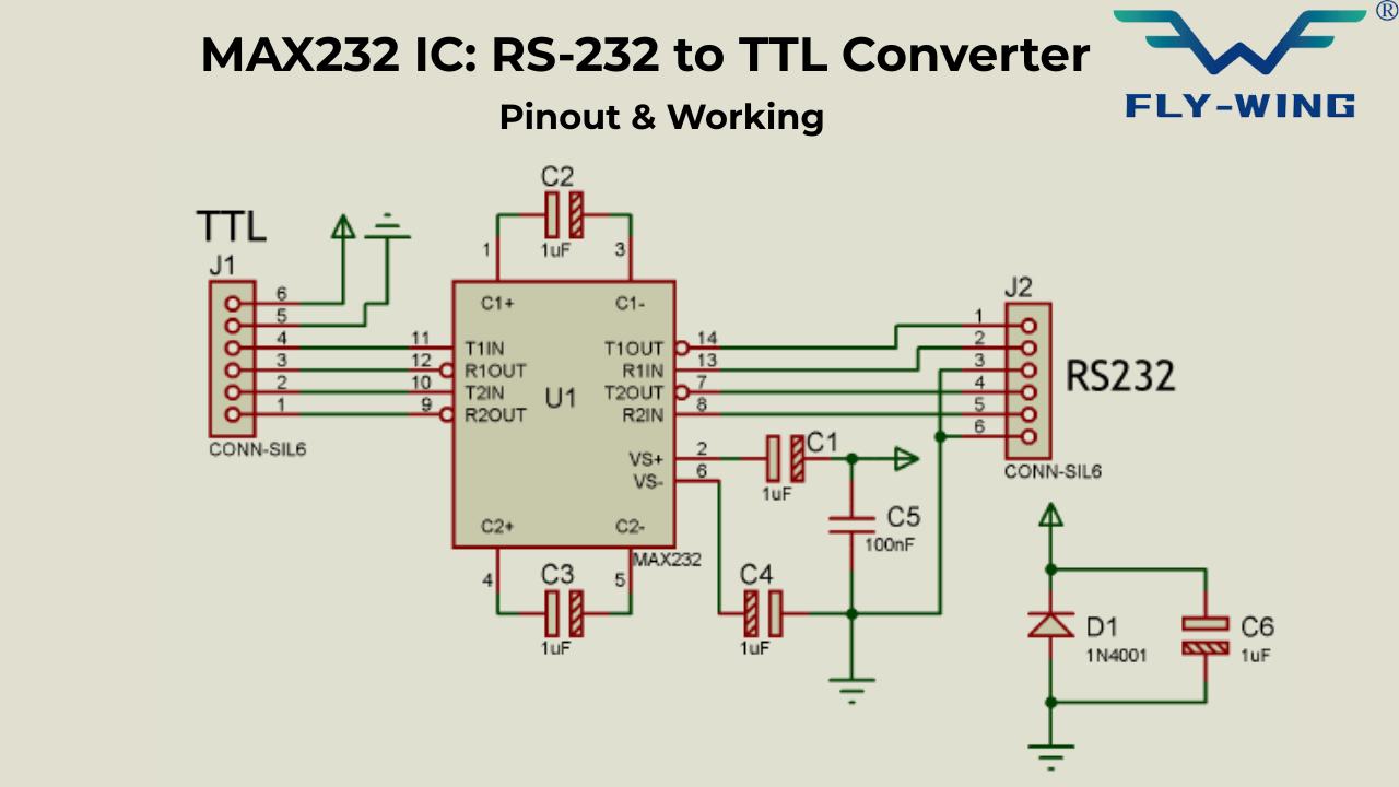
MAX232 Application Circuit: Wiring Step by Step
The complete application circuit for the MAX232 requires the IC itself, four capacitors, a 0.1 µF VCC bypass capacitor, and the interconnections between the MCU UART and the DB9 connector. That is all. No additional active components are needed.
Component List for Minimal Circuit
- MAX232 IC (DIP-16 or SOIC-16)
- C1, C2 — 1.0 µF capacitors (flying capacitors for charge pump)
- C3 — 1.0 µF capacitor (V+ reservoir — connect positive terminal to pin 2, negative terminal to VCC)
- C4 — 1.0 µF capacitor (V− reservoir — connect positive terminal to GND, negative terminal to pin 6)
- C5 — 0.1 µF ceramic bypass capacitor (VCC to GND, as close to pin 16 as possible)
- DB9 female connector (for connection to PC or RS-232 equipment)
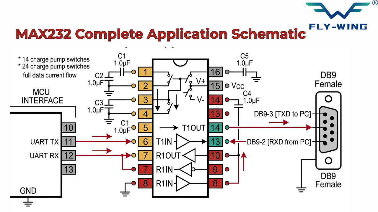
Step-by-Step Wiring: Primary Channel (TX/RX Data)
Follow this sequence for the primary communication channel. Work from the MCU side to the RS-232 side.
- MCU UART TX → MAX232 pin 11 (T1IN). This is the TTL transmit line from the microcontroller.
- MAX232 pin 14 (T1OUT) → DB9 pin 3. This is the RS-232 transmit line to the PC (TXD from device).
- DB9 pin 2 → MAX232 pin 13 (R1IN). This is the RS-232 receive line from the PC (RXD from PC).
- MAX232 pin 12 (R1OUT) → MCU UART RX. This returns the TTL receive signal to the microcontroller.
- DB9 pin 5 → circuit GND. Common ground reference is essential.
The signal inversion is automatic. You do not configure or program it. The MAX232 driver inverts the TTL signal to produce the correct RS-232 polarity, and the receiver inverts back. Your MCU firmware simply uses the UART normally.
Using the Second Channel for RTS/CTS Flow Control
Hardware flow control uses the RTS (Request to Send) and CTS (Clear to Send) lines. To implement it: connect MCU RTS GPIO → MAX232 pin 10 (T2IN) → pin 7 (T2OUT) → DB9 pin 7 (RTS). Connect DB9 pin 8 (CTS) → MAX232 pin 8 (R2IN) → pin 9 (R2OUT) → MCU CTS GPIO. This mirrors the primary channel wiring exactly, using channel 2 instead of channel 1.
PCB Layout Guidelines
Place C1, C2, C3, and C4 as close to the MAX232 as the layout allows. The charge pump traces carry switching current; long traces add parasitic inductance that degrades charge pump efficiency and increases noise. Keep RS-232 traces (pins 7, 8, 13, 14) physically separated from TTL signal traces to minimize crosstalk. Add the 0.1 µF bypass capacitor on pin 16 with a via directly to the ground plane.
C1: Positive → Pin 1, Negative → Pin 3
C2: Positive → Pin 4, Negative → Pin 5
C3: Positive → Pin 2, Negative → VCC (NOT GND — see previous warning)
C4: Positive → GND, Negative → Pin 6
Note: Non-polarized ceramic capacitors are strongly recommended for C1 and C2 because they eliminate orientation errors and improve reliability.
MAX232 Application Domains
MCU-to-PC Serial Communication
This is the most common application of using a MAX232. An embedded firmware-based microcontroller that’s trying to interface with a PC (to log data, debug, control, etc.) will have either a physical COM port or a USB to RS-232 converter connected to the PC. The MAX232 converts the voltage levels between the embedded firmware-based microcontroller’s UART (Universal Asynchronous Receiver Transmitter) and the exact DB9 connector that the cable will connect into on the PC.
For Arduino board users: The Arduino Uno includes an onboard USB-to-serial chip (ATmega16U2 or CH340, depending on the revision), so you only need the MAX232 when you connect to a real RS-232 device or to a PC with a physical RS-232 port, not when you use the Arduino’s native USB port.
For STM32, PIC, and AVR-based microcontrollers that do not have onboard USB, the MAX232 provides a simple path to connect to a PC serial terminal for debug output. You simply configure the UART on the microcontroller to 9600 or 115200 baud and connect from the microcontroller’s UART to a DB9 cable using the MAX232, and then use PuTTY or Tera Term from your PC.
Industrial Equipment and PLC Interfaces
Manufacturers design many industrial devices such as PLCs, motor controls, barcode scanners, weighing systems, and older HMI terminals for long service life, and these devices still use RS-232 for configuration and communication. Because they have a very long life span, these devices have RS-232 connectors (serial) that will outlive both the device itself and the life of the embedded device in which they reside.
When you connect an embedded microcontroller to these devices using RS-232, you generally need a voltage translation device such as the MAX232 on the embedded side. The MAX232’s input tolerance rating (±30 V) helps protect against input voltages that may exceed TTL levels due to ground potential differences over long industrial cable runs.
GPS Receiver Interfacing
Many GPS receivers (industrial and automotive), and most of the older models of GPS receivers, as well as those intended for use in marine and aviation environments, generally have an output of NMEA sentence data in RS-232 level voltages and at either a 4800 or 9600 baud rate. Therefore, if you are using a TTL-level MCU, then you must use a MAX232 IC RS-232 TTL converter on the receive side of the GPS.
Receiving from GPS is generally the only thing that you will need: the MCU listens to the GPS NMEA output. Use 1 of the 2 receiver channels available on the MAX232 and leave the other receiver channel of the MAX232 empty; connect the (T1IN, T2IN) unused transmitter inputs to VCC or GND will NOT leave them open or floating.
Cable Length Considerations
RS-232 is a single-ended standard. It is susceptible to noise on longer cable runs. The standard allows approximately 15 meters of cable at 9600 baud. In practice, well-shielded cable in low-noise environments can run longer. At higher baud rates, maximum cable length decreases — roughly inversely proportional to baud rate.
For cable runs beyond 15 meters, RS-485 is the correct choice. RS-485 uses differential signaling, which rejects common-mode noise. It supports cable runs up to 1200 meters at low baud rates. A MAX485 or similar differential driver/receiver replaces the MAX232 for these applications.
MAX232 vs. MAX3232 vs. MAX232A: Engineering Selection Guide
The MAX232 family has several variants. Choosing the wrong one for your supply voltage or application will cause the circuit to fail or perform below specification. This is not an upgrade path — it is a functional selection based on your design constraints.
| Parameter | MAX232 | MAX232A | MAX3232 | ST3232 |
|---|---|---|---|---|
| Supply Voltage | 5 V only | 5 V only | 3.0–5.5 V | 3.0–5.5 V |
| Cap Value (C1–C4) | 1.0 µF | 0.1 µF | 0.1 µF | 0.1 µF |
| Max Data Rate | 120 kbps | 120 kbps | 120 kbps | 250 kbps |
| Sleep Current | N/A | N/A | ~1 µA | ~1 nA |
| ESD (HBM) | 2 kV | 2 kV | ±15 kV | ±15 kV |
| Operating Temp. | 0–70°C | 0–70°C | −40–85°C | −40–85°C |
| Best For | Legacy 5V systems | Legacy 5V, smaller caps | New 3.3V/5V designs | Battery & high speed |
Why MAX232 Fails at 3.3 V
A 5V power supply is required for the MAX232 charge pump to create a proper RS-232 output voltage. At 3.3V, the voltage doubler and inverter will only generate +6.6V and -6.6V, respectively. RS-232 has a minimum requirement of ±5V at load; thus, when supplied with 3.3V power, there is not going to be sufficient margin, and the actual output levels will fall below specification with any reasonable capacitive or resistive load connected to the RS-232 line.
So if you need to connect a 3.3V MCU to a standard MAX232 interface, you should provide a separate 5V power supply to the MAX232 while maintaining the TTL parameters for your interface at 3.3V. In doing so, R1OUT (MAX232 receiver output) will be approximately 3.5V high, which should fall well within the input tolerance of most 3.3V MCUs. A more appropriate solution is to simply use the MAX3232.
Pin-Compatible Clones
Several manufacturers produce direct pin-for-pin and function-for-function replacements for the MAX232. These are fully interchangeable in most circuits. Common examples include: ICL232 (Renesas/Intersil), SP232 (Sipex/Exar), ST232 (STMicroelectronics), ADM232 (Analog Devices), and HIN232 (Harris/Intersil).
One caution: always verify the C3 connection requirement for any specific manufacturer’s variant before using it in a circuit designed for the original Maxim chip. The TI/Maxim difference described in Section 5 may apply to other clones as well. When in doubt, connect C3 to VCC — this is safe for all known variants.
When to Use RS-485 Instead
RS-232 works on a point-to-point basis; there is one transmitter and one receiver, and there is only one cable. The RS-485 standard allows a single bus to accommodate up to 32 driver/receiver pairs. If you want to connect multiple devices to the same serial connection, you are on an RS-485; RS-232 cannot do this. RS-485 also provides much greater distance between devices than RS-232, and it has a high degree of noise immunity within the industrial environment.
If you have an RS-232 cable with a need for extension, you can connect it using RS-485 converters. This consists of a MAX232 to convert TTL to RS-232 at one end of the cable; at the opposite end of that cable, a MAX485 will convert from RS-232 to RS-485 differential. The opposite conversion can be done at the receiving application. Though this is an uncommon application, it is effective.
Troubleshooting Common MAX232 Problems
Most MAX232 circuit failures fall into four categories. Each has a distinct diagnostic signature and a direct fix. Working through them in order usually identifies the fault within minutes.
IC Gets Hot Immediately After Power-On
The main reason for the occurrence of this problem usually involves the grounding of capacitor C3 in some versions of MAX232 ICs produced by Maxim Integrated. In such conditions, the internal charge pump will try to work in accordance with an inaccurate reference circuit, resulting in unnecessary energy consumption and overheating of the chip.
It is necessary to turn off the power right away to prevent irreversible consequences.
First, one needs to find out the real producer of the chip using packaging symbols and procurement information. In the case of Maxim Integrated, one needs to disconnect C3 from ground and connect it to VCC according to the proper configuration. In cases where no manufacturer information is available, you can assume that any producer’s chip uses the configuration with C3 connected to VCC.
Garbled Characters or No Data at All
This symptom usually points to one of three causes. First: wrong capacitor values. Using 0.1 µF capacitors with an original MAX232 (not the A variant) leaves the charge pump under-loaded, and V+ / V− rails droop under current draw. The RS-232 output drops below the ±5 V minimum. Use 1.0 µF for the original MAX232.
Second: reversed polarity on electrolytic capacitors. A reversed capacitor does not charge correctly — it may show high leakage or damage itself. Check each capacitor against the pinout table and replace any that were installed backwards.
Third: missing or inadequate VCC bypass capacitor. The charge pump injects switching noise back into the VCC rail. Without a 0.1 µF ceramic bypass cap on pin 16, this noise can corrupt the TTL logic and produce intermittent data errors.
No RS-232 Output Signal
If there is a valid TTL signal on T1IN but no RS-232 signal on T1OUT, check the charge pump rails first. Measure V+ (pin 2) and V− (pin 6) with a DMM. V+ should read approximately +8 V to +10 V. V− should read approximately −8 V to −10 V. If either rail is missing, the capacitors or their connections are the problem.
If the rails are correct, check the TX/RX wiring direction. The T1IN pin must receive an active TTL signal; a floating input produces an indeterminate output. Also verify that the MCU UART is actually transmitting. A simple LED blink on a spare GPIO, synchronized with data transmission, confirms the MCU is running.
Oscilloscope Verification: What to Look For
T1IN (pin 11) has a TTL UART signal varying between 0 volts and approximately 3.3-5 volts, with the idle state being high (5 volts). The start bit brings the line to a low state. The data bits follow at the speed chosen for communication (baud rate).
T1OUT (pin 14) outputs the same data pattern, but the system inverts it and level-shifts it downward. This pin remains in a negative idle state (approximately -7.5 V), and when it sends the start bit, it produces a positive pulse (approximately +7.5 V). The available amplitude must be a minimum of +/- 5 volts when measured while under load.
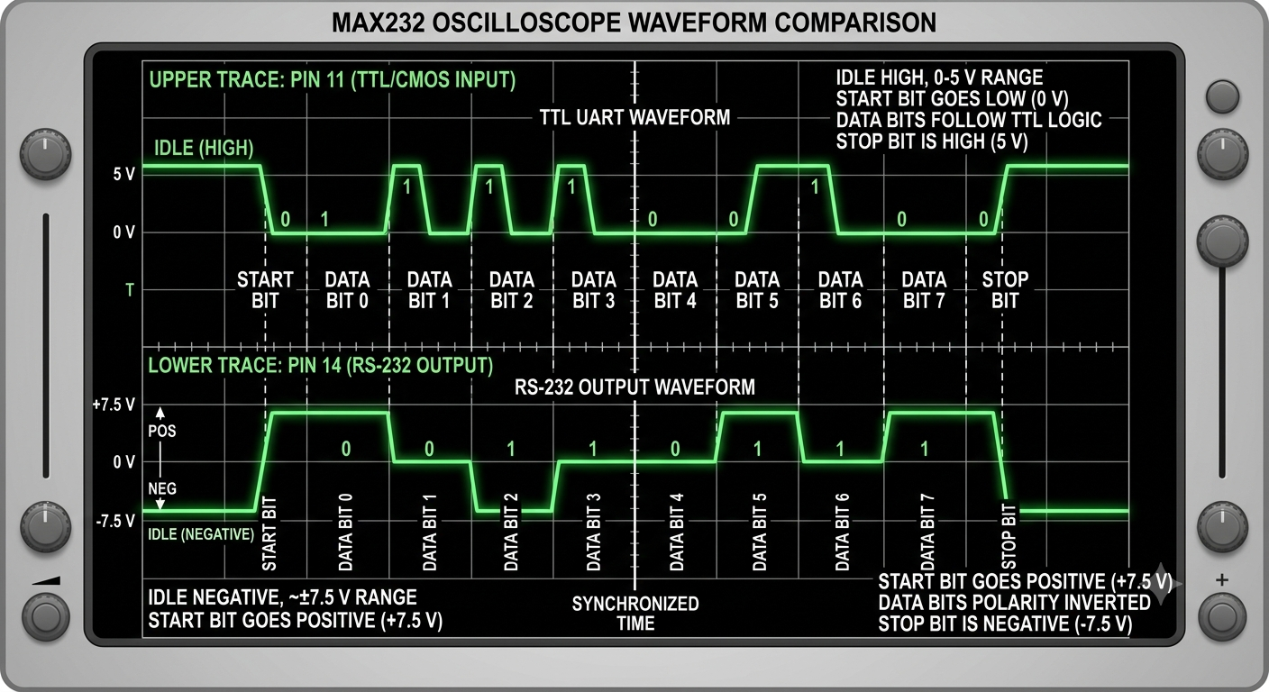
If T1OUT shows a signal but the PC receives no data, check for a crossover. The modem connects the T1OUT pin to pin 3 (TD) on the DB9 cable at the device. The PC should be receiving data through RD on pin 3 (DB9) from its perspective. A standard DB9/F to DB9/F cable connects pin 3 to pin 3, so pin 3 at one end of the cable connects directly to pin 3 at the other end in normal (non-null modem) wiring. With a null modem cable, pin 2 of one connector connects to pin 3 of another — hence the extra inversion in the cabling.
Frequently Asked Questions
The MAX232 converts TTL/CMOS logic levels (0–5 V) to RS-232 voltage levels (±7 V approx.) and vice versa using an internal charge pump powered by a single +5 V supply.
The original MAX232 uses four 1.0 µF capacitors, while MAX232A and MAX3232 use smaller 0.1 µF capacitors. Ceramic or tantalum types can be used.
No. The MAX232 requires a 5 V supply. For 3.3 V systems, use the MAX3232, which supports 3.0–5.5 V operation.
MAX3232 supports lower voltage (3.0–5.5 V), uses smaller capacitors, and offers better ESD protection. MAX232 works only at 5 V but both are pin-compatible.
Modern USB-based systems use it less often, but industrial equipment such as PLCs and legacy devices still widely use it with RS-232 ports.
This is often due to an incorrect C3 capacitor connection. Some versions require C3 to be connected to VCC instead of GND, depending on the manufacturer.
Conclusion
Microcontrollers often need to communicate with serial devices such as RS-232 interfaces. One of the most commonly used devices for converting between TTL/CMOS logic and RS-232 voltages is the MAX232 IC. The MAX232 will take a +5V power supply, generate the required negative voltage from an internal charge pump, and provide the low and high signals to the RS-232 device. The MAX232 is popular because it is easy to integrate into embedded systems.
In this guide, we covered how to use the MAX232 chip by discussing how it works, its pinout and electrical characteristics, how the internal charge pump works, and other important design considerations such as what capacitors to use, how fast (baud rate) you can send data over the RS-232 interface, and possible differences between manufacturers.
Although modern communication has largely shifted toward USB-based interfaces, the MAX232 remains highly relevant in industrial and legacy systems such as PLCs, GPS modules, and older control equipment. Its reliability, standard compliance, and long-term availability make it a trusted solution in many engineering applications.
COMMENTS