Energy-harvesting power management ICs (PMICs) like the LTC3108 allow for the creation of battery-free electronic devices by converting ultra-low ambient energy into regulated power. While once restricted to university labs, these ICs are now advanced enough that a maker with a soldering iron and a $10 Thermoelectric Generator (TEG) can build a wireless sensor node in a single day.
The LTC3108, originally from Linear Technology (now Analog Devices), is the industry-standard “cold-start” harvester. Its ability to start from as little as 20 mV—the temperature gradient of a human handmakes it the de facto choice for industrial IoT, wearables, and edge computing. In this deep-dive, we analyze the LTC3108 internal architecture, compare it against competitors like the BQ25570, and provide five field-tested project schematics for your next batteryless design.
This article explains how the IC actually works and its performance in comparison to alternative energy harvesting ICs, and presents five practical projects built around the device.
Why Battery-Free Electronics Are Now Practical
The ambient energy landscape: sources and what they actually deliver
Ambient energy harvesting takes advantage of existing energy sources within the surrounding environment, such as differences in temperature, light, vibration, and RF fields. While none of these sources are as energy-dense as the lithium-ion batteries, they can still provide sufficient power for devices that only transmit small amounts of data.
The table below outlines common energy-harvesting sources, their typical real-world energy densities, and families of integrated circuits best suited to those harvesting technologies. The energy densities come from MDPI Energies publications and Analog Devices application notes.
Where energy-harvesting ICs fit in the signal chain
| Source | Typical Transducer | Typical Output Voltage | Outdoor / Industrial | Indoor Power Density | Suitable ICs |
|---|---|---|---|---|---|
| Thermal (TEG) | Peltier cell acting as TEG | 20–500 mV | Up to 1 mW/cm² (industrial heat) | 25–100 µW/cm² | LTC3108, LTC3109, BQ25570 |
| Solar / PV | Monocrystalline small cell | 0.4–5 V | 100+ µW/cm² (outdoor) | 10–100 µW/cm² (fluorescent) | SPV1050, BQ25570, MAX20361 |
| Piezoelectric | PZT cantilever | AC, 1–50 V peak | 1–3 mW near machinery | 4–500 µW (vibration dependent) | LTC3588-1, BQ25570 |
| RF Energy | Rectenna / dipole | 100–500 mV rectified | Up to 100 µW near 5G base stations | 0.1–10 µW at 1–3 m | P2110, Powercast P21XXCSR |
| Electromagnetic Induction | Current transformer (CT) | 0.5–5 V AC | Up to 2 mW from 100+ A lines | 50–500 µW from 5 A lines | LTC3108, custom bridge |
Raw signals from the transducers cannot be used. For example, a TEG may generate 80 mV at a 50 mA short circuit current; however, any practical digital system requires a regulated supply voltage like 3.3 V or 2.2 V. The energy harvesting IC bridges this gap by amplifying the millivolt input, managing a storage component, and giving out a regulated output with signaling for power good status.
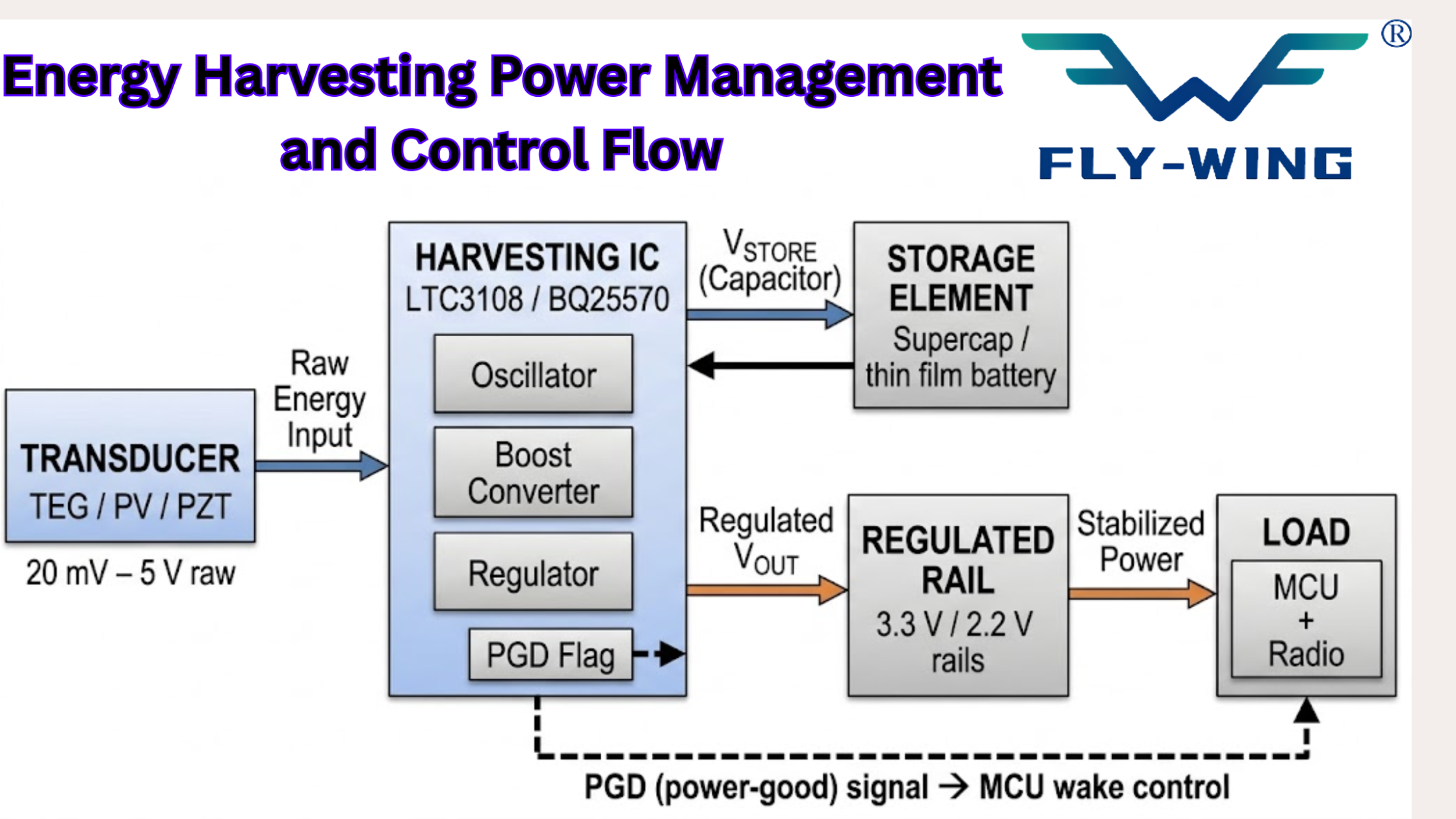
Inside the LTC3108: Architecture and Working Principle
The LTC3108 DC/DC converter manufactured by Analog Devices is designed specifically to extract and convert energy from very low-voltage power sources such as TEGs, thermopiles, and small photovoltaic cells. A clear understanding of its internal architecture is essential before beginning any circuit design.
Armstrong oscillator topology: bootstrapping from 20 mV
The question of system start-up if input voltage is not sufficient for powering ordinary CMOS logic is one of the most essential issues associated with the design of harvesting circuits. The LTC3108 solves this problem by means of applying a resonant step-up topology that exploits the Armstrong oscillator technique.
A step-up transformer with an external turns ratio (typically 1:100 with a minimum voltage input) is connected between VIN and SW pins of the chip. The latter provides a resonant oscillator which is constructed by means of utilizing a primary coil of a transformer along with a capacitor (C1; typical values 4.7-10 nF). With each cycle of the resonance procedure, the secondary side of the transformer multiplies the voltage so much that the diodes get forward-biased. Current rectification is conducted to VAUX. When VAUX equals approximately 0.5V (the threshold level that can be identified by the IC itself), a standard boost conversion procedure is carried out.
Thus, as we can conclude from the above discussion, the cold start-up from as low as 20mV is accomplished via a two-step procedure (oscillator → boost regulation) where the first stage requires minimal currents due to the resonance circuitry.
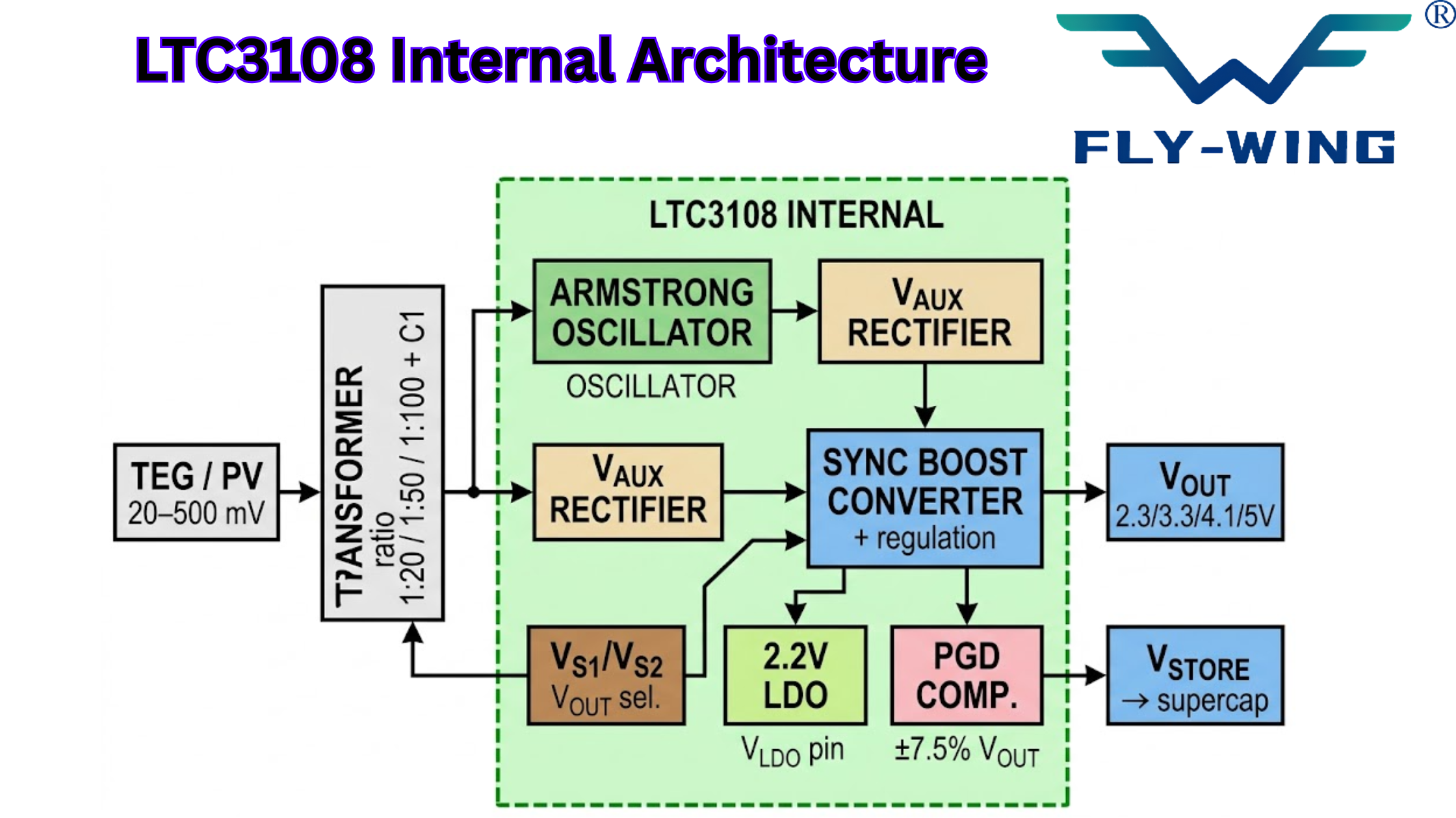
Synchronous boost converter: VOUT regulation and output sequencing
When sufficient charge exists on VAUX, the IC will transition from charging VAUX to operating as a boost converter. Internally, MOSFET switches will control the flow of energy out of VAUX to the VOUT capacitor. The output voltage delivered to the load is determined by two external pins (VS1 & VS2), which are selected by a resistor-trimmed internal reference. There is no external feedback resistor divider circuit; therefore, the four voltage options available are hard-programmed into the IC, thus simplifying layout by removing any potential for output voltage drift due to resistor tolerances.
The order of output voltage power-up is via sequencing as follows after a cold-start sequence: VAUX charges first, then 2.2V LDO (VLDO) powers up, then VOUT will power up to its programmed output voltage, and finally, the excess energy will discharge into VSTORE. Once VOUT has reached 7.5% from the target, PGD will go high, providing an indication to the MCU that it is safe for operation to begin.
VSTORE: energy buffering and blackout operation
The VSTORE pin is connected to the supercapacitor that serves as the external energy storage device (ESD), typically ranging from 100 µF to 0.1 F. When VAUX is present, VSTORE will be charged by the IC, but this charging is the secondary priority compared to VAUX charging. If the harvesting source is not present, such as when a TEG stops receiving its thermal energy source, the IC automatically turns to VSTORE to regulate VOUT. This switchover occurs seamlessly without the need for any external control circuitry.
LTC3108 vs LTC3108-1: which variant to choose
The LTC3108 and LTC3108-1 devices have the same pin layout, but their VS1/VS2 programming tables have been mapped to different output voltages. The LTC3108 provides four different output levels (2.3V, 3.3V, 4.1V, & 5V), while the LTC3108-1 has four other output levels (2.5V, 3.0V, 3.7V, & 4.5V).
Therefore, the LTC3108 is best suited for a load requiring a 3.3V output voltage (this is typically the most common voltage in today’s microcontrollers). Conversely, if your load is a radio or sensor that requires either a 3.0V or 3.7V output voltage (for example, some Bluetooth low energy or BLE), or if your load is going to charge a lithium-ion (Li-Ion) battery at up to 4.2V, you will be best off using the LTC3108-1.
LTC3108 Pin Reference and VOUT Configuration
The following table consolidates pin functions from the ADI LTC3108 datasheet (Rev. D). This is the most concise single-page reference available for design work.
LTC3108 Pin Function Reference
VOUT Voltage Selection — VS1 & VS2 Pin Programming
Energy-Harvesting IC Landscape: LTC3108 vs BQ25570 vs SPV1050 and Others
The LTC3108 is not the only chip available, and sometimes, it may not be the best one to choose. Since 2020, the options for ICs that can be used for energy harvesting have expanded drastically, and picking the wrong chip can make energy generation 30–50% less efficient.
| IC | Manufacturer | Min Cold-Start | MPPT | Best Source | VOUT Range | Quiescent IQ | Package |
|---|---|---|---|---|---|---|---|
| LTC3108 ★ Featured IC | Analog Devices | 20 mV | ✗ | TEG, thermopile, small PV | 2.3–5 V (fixed 4) | ~6 µA | DFN-12 / SSOP-16 |
| LTC3109 | Analog Devices | 30 mV | ✗ | TEG (bipolar / AC input) | 2.35–5 V (fixed 4) | ~6 µA | SSOP-20 |
| BQ25570 | Texas Instruments | 100 mV | ✓ programmable | Solar, TEG, piezo | 1.8–5.5 V (adj.) | ~330 nA | QFN-20 (3.5×3.5 mm) |
| SPV1050 | STMicroelectronics | 50 mV | ✓ resistor-set | Solar + TEG dual | 1.8 V, 3.3 V LDOs + unreg. | ~8 µA | QFN-20 (4×4 mm) |
| AEM20940 | e-peas | 50 mV | ✓ internal | Solar, TEG, RF | 1.2–4.5 V (adj.) | ~800 nA | QFN-24 (4×4 mm) |
| EM8900 | EM Microelectronic | 5 mV Lowest in class | ✗ | TEG (ultra-low gradient) | 1.2–3.3 V | ~400 nA | WLCSP (ultra-small) |
Texas Instruments BQ25570
The BQ25570 has utilized a completely different method than previous designs. Instead of utilizing an Armstrong Oscillator to generate the output voltage, it employs a nano-power hysteretic boost converter that has the ability to cold-start at 100 mV (or 50 mV with MPPT pre-bias).
What distinguishes the BQ25570 from other devices is its integrated Maximum Power Point Tracker (MPPT). In essence, when connected to a power source via the OC_SEP pin, the IC samples the power source’s open circuit voltage (Voc) continuously and always adjusts its working point in order to draw the maximum available power from the power source. As a result of this capability, the BQ25570 improves efficiency significantly when solar panels are used as a power source, since solar panels have a non-linear I-V curve based on the amount of light and temperature they are under during operation.
Additionally, the BQ25570 has a quiescent current of approximately 330 nA versus the LTC3108 with an approximately 3 µA quiescent current; thus, making it much more suitable for use in always-on monitoring applications.
When to choose BQ25570 over LTC3108: Your source is primarily solar, your available input is above 100 mV, and maximizing harvested watts matters more than cold-start voltage.
STMicroelectronics SPV1050
The SPV1050 is specifically intended for use in applications where simultaneous energy harvesting from two distinct types of energy sources (for example: A photovoltaic cell paired with a thermoelectric generator) is desired. The device features two independent regulated LDO outputs (1.8 V and 3.3 V) as well as an unregulated output stage, and it is configured to provide maximum power point tracking (MPPT) remotely using an external resistor divider. This capability provides flexibility so MPPT can be adjusted based on the characteristics of the solar panel used in the application. Additionally, both end-of-charge thresholds and under-voltage lockout thresholds can be externally trimmed for direct connection to thin-film batteries.
e-peas AEM20940 and EM Micro EM8900
In cases where the temperature difference between the hot and cold sources is very low, such as in body-worn energy harvesters with less than 2°C difference between skin and air temperatures, the EM8900 will function using an input voltage as low as 5 millivolts. The AEM20940 IC offers cold start operation below 50 millivolts, as well as three different modes of energy harvesting.
IC Selection Decision Guide
Selecting the right energy-harvesting IC depends on the input source, startup voltage requirements, and efficiency priorities. The following guide summarizes the most suitable choices based on application needs:
Pairing the LTC3108 with Real-World Energy Sources
Thermoelectric generators: what the datasheet does not tell you
Choosing a TEG for use with the LTC3108 involves a compromise between three conflicting characteristics: Seebeck coefficient (V/K), source resistance (Ω), and size. Notably, the data sheet of the LTC3108 specifies source resistance ≤ 3 Ω for efficient power generation. The source resistance of miniature Peltier coolers used as TEGs is in the range 1-4 Ω, depending on temperature. Source resistance should be measured at the actual working temperature and not at room temperature.
A 40 mm × 40 mm TEG with a temperature difference of 10°C across its surfaces produces about 4 mW when optimally matched for the LTC3108 application, which would be enough to power a wireless temperature logger taking measurements every five minutes. In order to keep the temperature difference of 10°C, proper heatsinking is necessary on the side exposed to lower temperatures. Without a heatsink, the temperature difference collapses to 2-3°C due to convective losses.
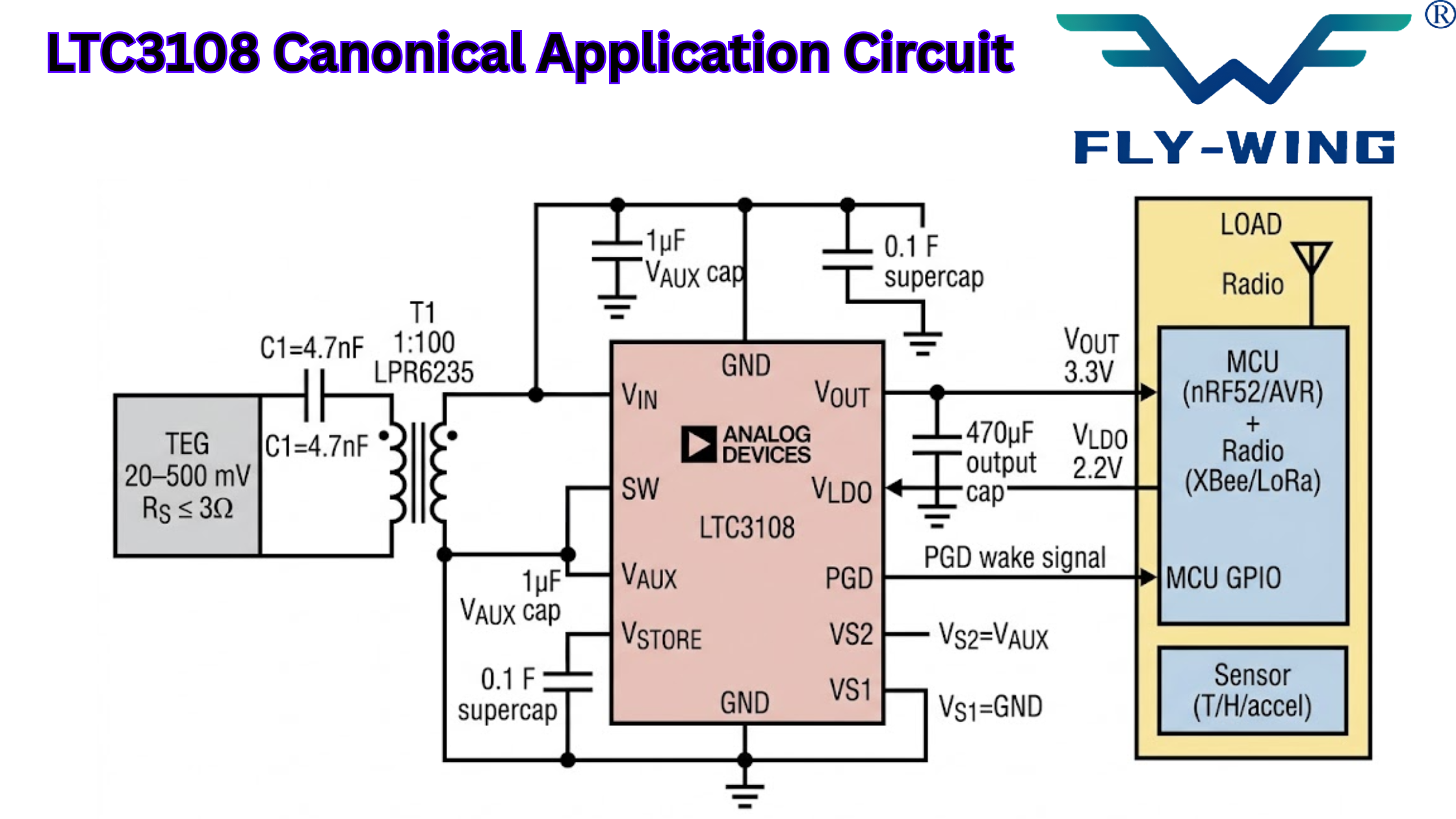
Transformer selection for the LTC3108
The transformer is the single most performance-critical external component. ADI recommends three transformer options depending on the input voltage range:
| Source | Typical Transducer | Typical Output Voltage | Outdoor / Industrial | Indoor Power Density | Suitable ICs |
|---|---|---|---|---|---|
| Thermal (TEG) | Peltier cell acting as TEG | 20–500 mV | Up to 1 mW/cm² (industrial heat) | 25–100 µW/cm² | LTC3108, LTC3109, BQ25570 |
| Solar / PV | Monocrystalline small cell | 0.4–5 V | 100+ µW/cm² (outdoor) | 10–100 µW/cm² (fluorescent) | SPV1050, BQ25570, MAX20361 |
| Piezoelectric | PZT cantilever | AC, 1–50 V peak | 1–3 mW near machinery | 4–500 µW (vibration dependent) | LTC3588-1, BQ25570 |
| RF Energy | Rectenna / dipole | 100–500 mV rectified | Up to 100 µW near 5G base stations | 0.1–10 µW at 1–3 m | P2110, Powercast P21XXCSR |
| Electromagnetic Induction | Current transformer (CT) | 0.5–5 V AC | Up to 2 mW from 100+ A lines | 50–500 µW from 5 A lines | LTC3108, custom bridge |
5 Maker Projects Using Energy-Harvesting ICs
Each project below contains a minimal bill of materials and a power budget table. Consequently, power budgets are estimated based on the target duty cycle. All the components are forecasted to be in production by 2025 and available at Fly-Wing Tech.
The small TEG (15 mm × 15 mm, e.g., Laird UTG-57-40-F2) is placed onto the wrist using a clamp with low thermal resistance. The temperature of the skin (~34°C) and environment (~22°C) results in ~12°C dT. For 15 mm TEG operating with this dT, about 80–150 µW of power can be produced, dependent on the quality of the heatsink. After that, once the supercapacitor is charged by the LTC3108, the nRF52840 wakes up from the System OFF mode.
Power Budget — Project 1
| Component | State | Current | Duration / Duty | Average Power |
|---|---|---|---|---|
| nRF52840 | System OFF sleep | 0.4 µA | ~59.5 sec | 0.4 µW @ 3.3 V |
| nRF52840 | Active + BLE TX | ~7 mA peak | ~500 ms per min | ~58 µW avg |
| SHT31 sensor | Measure + idle | 0.2 µA idle / 1.5 mA meas. | 2 ms measure | ~0.1 µW avg |
| LTC3108 | Quiescent (always on) | ~6 µA @ VIN | Continuous | ~0.3 µW |
| Total average | — | — | — | ~59 µW |
| TEG available | 12°C dT, 15 mm TEG | — | — | 80–150 µW |
BUILD NOTE
Use the VOUT2_EN pin to disconnect the nRF52840’s VDD entirely between transmissions. This reduces system sleep current to the LTC3108 quiescent + SHT31 idle only (~6.6 µA total). The PGD pin connected to the nRF52840 P0.04 GPIO triggers wakeup in under 10 µs.
MPPT CONFIGURATION NOTE
Set the BQ25570 MPPT ratio to 80% by selecting R_OC1 and R_OC2 per the TI datasheet calculator. For the IXYS SLMD121H10L, an MPPT voltage of approximately 2.4 V (80% of ~3 V VOC at 300 lux) is optimal. The reference design is the TI TIDA-00242 evaluation board.
IMPORTANT: RESONANCE MATCHING
A piezoelectric cantilever only harvests efficiently when its natural resonant frequency matches the vibration source. Verify the vibration spectrum of your target machine with an accelerometer log before sizing the cantilever. A 2 Hz mismatch between cantilever resonance and source frequency can reduce output power by over 80%.
Power Budget — Project 4
| Component | State | Current | Duration | Average Power |
|---|---|---|---|---|
| SAMD21 | Standby sleep | 5 µA | ~299.8 sec / 5 min | 16.5 µW |
| SAMD21 | Active (wake + compute) | 3 mA @ 3.3 V | ~200 ms | 6.6 µW avg |
| SX1262 | LoRa TX (14 dBm) | ~87 mA | ~150 ms | ~435 µW avg |
| LTC3108 | IQ (always on) | 6 µA @ VIN | Continuous | ~0.5 µW |
| Total average | — | — | — | ~459 µW |
| TEG harvest | 40 mm, 35°C dT | — | — | ~14,000 µW |
THIN-FILM BATTERY VS. SUPERCAPACITOR
For multi-day outages (cloudy agricultural environments), a thin-film LiPON battery is preferred over a supercapacitor because its self-discharge rate is measured in months, not days. The SPV1050 supports direct thin-film battery charging with adjustable end-of-charge voltage — set VEOC to 4.1 V for extended cycle life. Supercapacitors discharge ~20% per day in typical ambient conditions.
Critical Design Pitfalls and How to Fix Them
Pitfall 1: Wrong transformer or leakage inductance too high
Problem: The circuit fails to oscillate or oscillates poorly, and VAUX never charges above 0.3 V despite a valid VIN signal.
Root cause: The transformer’s leakage inductance is too high relative to its magnetizing inductance, or the winding capacitance is resonating at a frequency the LTC3108 cannot track. Substituting a generic audio transformer with unmeasured winding capacitance causes this.
Fix: Use only the Coilcraft or Würth transformers from ADI Table 5. Measure leakage inductance with an LCR meter before populating. Do not substitute similar-value inductors — the turns ratio and core material matter critically.
Pitfall 2: High-leakage storage capacitor draining VSTORE overnight
Problem: The sensor node worked during initial testing (continuous harvesting) but fails to restart after an overnight shutdown period.
Root cause: Generic aluminum electrolytic capacitors have leakage currents of 10–100 µA at rated voltage, which outpaces the trickle charge available from a small TEG in a low-gradient environment. The supercapacitor drains completely before morning.
Fix: Use low-leakage supercapacitors — ADI’s Table 6 recommends Panasonic EECEN series or AVX TPSX series. Measure actual leakage at the operating voltage, not at rated voltage.
Pitfall 3: Brown-out reset loop due to incorrect PGD-pin usage
Problem: The MCU boots, begins transmitting, then resets repeatedly in a fast loop, consuming more power than harvested and preventing VOUT from ever stabilizing.
Root cause: The MCU is waking on PGD rising edge but starting its radio immediately at full power, collapsing VOUT below the LTC3108 regulation band, pulling PGD low, causing a reset, and repeating.
Fix: After PGD goes high, add a firmware delay of 200–500 ms before enabling the radio, allowing VOUT to charge to full regulation. Also size the VOUT capacitor for the maximum expected load current burst:
$C = I_load × t_burst / ΔV_allowed.$
For a 90 mA radio burst over 150 ms with 200 mV tolerable droop:
$C = 0.09 × 0.150 / 0.200 = 67.5 mF.$
Use a 100 mF VOUT capacitor for this load.
Pitfall 4: PCB layout resistance in the primary winding path
Problem: The circuit cold-starts at lab temperatures but fails below 10°C (reduced TEG output).
Root cause: High trace resistance between VIN, transformer primary, SW pin, and GND creates a voltage drop that effectively raises the minimum operational VIN. The IC can carry up to 500 mA in the switch path; even 10 mΩ of stray resistance creates a 5 mV drop at 500 mA, enough to prevent cold-start at marginal input voltages.
Fix: Route VIN, SW, and GND with minimum trace length, maximum width (≥ 1 mm for 1 oz copper on a two-layer board), and no vias in the primary path. Therefore, use a ground plane under the IC, and ensure the thermal pad is soldered in DFN-12 packages.
| Symptom | Root Cause | Fix |
|---|---|---|
| VAUX < 0.3 V | Wrong transformer / high leakage | Use Coilcraft / Würth specified part |
| Fails after long OFF | High-leakage supercap | Use Panasonic EECEN / AVX TPSX |
| MCU reset loop | Radio starts too early | Add 200–500 ms delay after PGD |
| Cold start <10°C fail | Trace resistance drops VIN | ≥1 mm trace, no vias, solid pad |
| Low efficiency | TEG RS > 3 Ω | Use TEG RS ≤ 2 Ω (measure hot) |
Simulating and Bench-Testing LTC3108-Based Circuits
LTspice simulation setup
Analog Devices provides an LTspice model for the LTC3108. After importing the model file (LTC3108.lib from the ADI website), the TEG can be modeled as a voltage source in series with a resistance matching the TEG’s internal source resistance. Use a Thevenin equivalent: V_TEG in series with R_source.
For the transformer, LTspice requires specifying both magnetizing inductance and the coupling coefficient. For the Coilcraft LPR6235 at 1:100 turns ratio, use L_primary = 47 µH, L_secondary = 470 mH, coupling coefficient K = 0.97. Specifically, winding resistance should be set to the measured DCR (typically 0.2 Ω primary, 18 Ω secondary for this part).
Bench measurement methodology
Measuring quiescent currents in the µA range requires a precision source-measure unit (SMU) or a high-sensitivity ammeter (Keithley 2450 or similar). Standard DMMs in series with the circuit introduce sufficient series resistance and voltage drop to disturb the measurement.
For cold-start characterization, use a precision DC power supply set to the target VIN (e.g., 50 mV), output impedance set to simulate the TEG source resistance (use a series resistor on the bench). Monitor VAUX, VLDO, and VOUT on separate oscilloscope channels to observe the startup sequencing described in the datasheet. Cold-start time from 20 mV with a 0.1 F supercapacitor is typically 60–180 seconds — be patient during initial characterization.
Evaluation board: ADI DC1582B-A
ADI offers the DC1582B-A evaluation board for the LTC3108 and the DC1582B-B for the LTC3108-1. These boards include jumper-selectable turns-ratio transformers, test points at every key node, and a header for connecting a Silicon Labs EFM32 Gecko starter kit as the load MCU. For initial feasibility testing with a new TEG source, evaluating this board before committing to a custom PCB layout saves significant debug time.
Energy Harvesting ICs in 2025–2026: Trends Makers Should Track
Sub-5 mV cold-start ICs: closing the gap on perpetual-energy devices
The EM Microelectronic EM8900, capable of cold-starting from 5 mV, opens applications where the LTC3108’s 20 mV threshold is a barrier — sub-1°C thermal gradient harvesting, very small body-surface TEGs, and harvesting from thermocouple arrays on room-temperature surfaces. As of 2025, the EM8900 is priced at approximately $0.79 in single quantities, making it accessible for maker projects.
Intermittency-aware computing frameworks
A fundamental challenge with energy-harvested systems is that power can disappear mid-computation. Research projects like Chinchilla (Berkeley) and the Rust-based iotedge-intermittent framework use non-volatile SRAM checkpointing to resume computation across power outages transparently. For maker projects, the simplest approach is designing firmware as a series of idempotent tasks: sense → store to EEPROM → transmit → sleep. Each stage is atomic; if power fails between stages, the next startup simply retries from the last committed EEPROM state.
Multi-source IC integration
The trend in commercial IoT deployments is toward ICs that handle two or three harvesting sources simultaneously solar by day, TEG from HVAC heat by night, and RF from a nearby access point as a backup. The e-peas AEM20940 supports this architecture natively. For makers, this trend means that a single-IC, multi-source board is now achievable without complex external power management logic.
Frequently Asked Questions
With a properly sized 40 mm × 40 mm TEG and good heatsinking, the LTC3108 can start from temperature differences as low as ~1°C (no-load). For practical operation with MCU and radio, a more realistic requirement is 5–10°C, depending on the TEG size and load.
No. The LTC3108 does not include Li-ion charging control (CC/CV). It should not be connected directly to a Li-ion cell. Instead, use a dedicated charger IC (e.g., MCP73831). For thin-film batteries, devices like the SPV1050 are more suitable.
The LTC3109 supports both DC and low-frequency AC inputs and can handle either polarity, making it suitable for more flexible TEG orientations. The LTC3108 only supports positive DC inputs. Both share similar ultra-low voltage cold-start behavior.
This usually happens when VOUT is loaded too early or too heavily. During startup, the IC prioritizes charging VAUX first. Also, high-leakage capacitors on VOUT can prevent proper charging. Ensure no load is connected during initial startup testing.
Yes, but it is not optimal. The LTC3108 does not include MPPT, so it cannot efficiently track a solar panel’s maximum power point. For solar harvesting, ICs like the BQ25570 or SPV1050 are better choices.
Conclusion
ICs for energy harvesting have emerged beyond the experimental stage to become available to makers. The LTC3108 continues to be the state-of-the-art device for ultra-low cold-start voltage (20 mV) for TEG and thermopile applications, featuring oscillator, boost converter, LDO, power-good indication, and storage control all in one tiny package of 3×4 mm.
If solar harvesting is the primary source, then the BQ25570 gives MPPT and less quiescent current with the trade-off of higher cold-start voltage. The most integrated circuit for hybrid source and thin film battery charging is the SPV1050, which does not require a separate charger IC.
Five projects that can be designed based on the guidelines presented in this guide span the realistic capability range of current ICs for harvesting: from several microwatts generated from body heat to tens of milliwatts generated from industrial sources. In each project, the design criteria are similar: minimize average power drawn through duty cycling, allocate storage sufficient for the outage period, and choose an IC configuration suitable for the power source.

COMMENTS