Introduction to LM723 Voltage Regulator
The LM723 is a monolithic integrated programmable voltage regulator, assembled in a 14-lead dual-in-line plastic package. It is capable of providing 2V-37V output voltage and delivering 150mA of output current. However, with the addition of an external transistor, it can provide an output current up to 10A. LM723 offers extremely low standby current drain and foldback current limiting features. A foldback current limiter in a circuit reduces the power supply output current when an overload condition occurs.
LM723 is widely used in a range of applications, including shunt regulators, current regulators, temperature controllers, battery chargers, microcontroller-based circuits, and adjustable and fixed power supplies. LM723 is a high-precision voltage regulator IC capable of delivering both positive and negative output voltages with exceptional stability and accuracy. Therefore, it is among the widely used voltage regulators in analog and power electronics. It also has a wide operating temperature over 0°C to +70°C. However, LM723C is the same as LM723 except for the fact that LM723C has a temperature operating range of −55°C to +125°C.
What is LM723 Voltage Regulator IC?
The LM723 or LM723C is a voltage regulator designed primarily for series regulator applications. It is an adjustable voltage regulator with a maximum input voltage of 40V and an output voltage between 2V and 37V. Unlike traditional regulator ICs such as 7805 and 7812, which only provide fixed output voltages and low output current. LM723 offers adjustable output voltage with a maximum of 10A output current. It can supply 150mA output current without an external pass transistor. However, with an external series pass transistor, LM723 can supply up to 10A of output current.
LM723 can be used either as a linear or a switching regulator. It also features a foldback current limiting circuit. Therefore, it can withstand overload conditions by reducing the output supply current. The LM723 provides both positive and negative voltage regulators, offering an adjustable output from 2V to 37V. LM723’s ability to provide adjustable voltages ranging from 2V to 37V and adjustable current with an external pass transistor up to 10A makes it a perfect choice for various analog and power electronic applications, including shunt regulators, battery chargers, and battery controllers.
LM723 comes in various packages, including PDIP and TO-100. The specific package can vary depending on the manufacturer and the temperature range the device is designed for. The most common manufacturers of LM723 are Texas Instruments (TI) and STMicroelectronics.
LM723 Pinout & Typical Packages
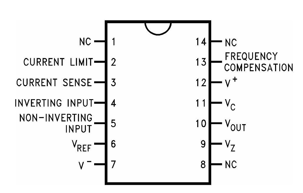
The LM723 Voltage Regulator IC features a total of 14 pins, each serving a specific function that contributes to its flexibility and precision in voltage regulation applications. Understanding the LM723 pinout configuration is crucial for achieving proper circuit design, stability, and optimal performance. Whether used in a series regulator, shunt regulator, or current limiter, each pin plays a vital role in defining the regulator’s output characteristics.
LM723 Pinout — Pin Functions
| PIN No. | Pin Name | Pin Function |
|---|---|---|
| 1 | NC | No internal connection |
| 2 | Current Limit | Used with a sense resistor for current limiting/foldback (base terminal of internal current limit circuit). |
| 3 | Current Sense | Used for current foldback applications (emitter of the current limit circuit). |
| 4 | Inverting Input | Inverting input of the internal error amplifier. |
| 5 | Non-inverting Input | Non-inverting input of the error amplifier (tie to VREF divider for setpoint). |
| 6 | Vref | Internal reference output (~7.15 V typical). Check the datasheet for limits. |
| 7 | V- (GND) | Negative supply/ground pin (0 V in single-supply use). |
| 8 | NC | No internal connection |
| 9 | Vz | Zener reference terminal — used for negative regulator setups. |
| 10 | Vout | Regulator output (internal or external pass transistor drive). |
| 11 | Vc | Collector connection for internal pass transistor drive. |
| 12 | V+ | Unregulated input / positive supply for the IC (up to 40 V max). |
| 13 | Frequency Compensation | Connect a small capacitor (~100 pF) to the inverting input for stability. |
| 14 | NC | No internal connection |
Always verify with the official LM723 datasheet before design or testing.
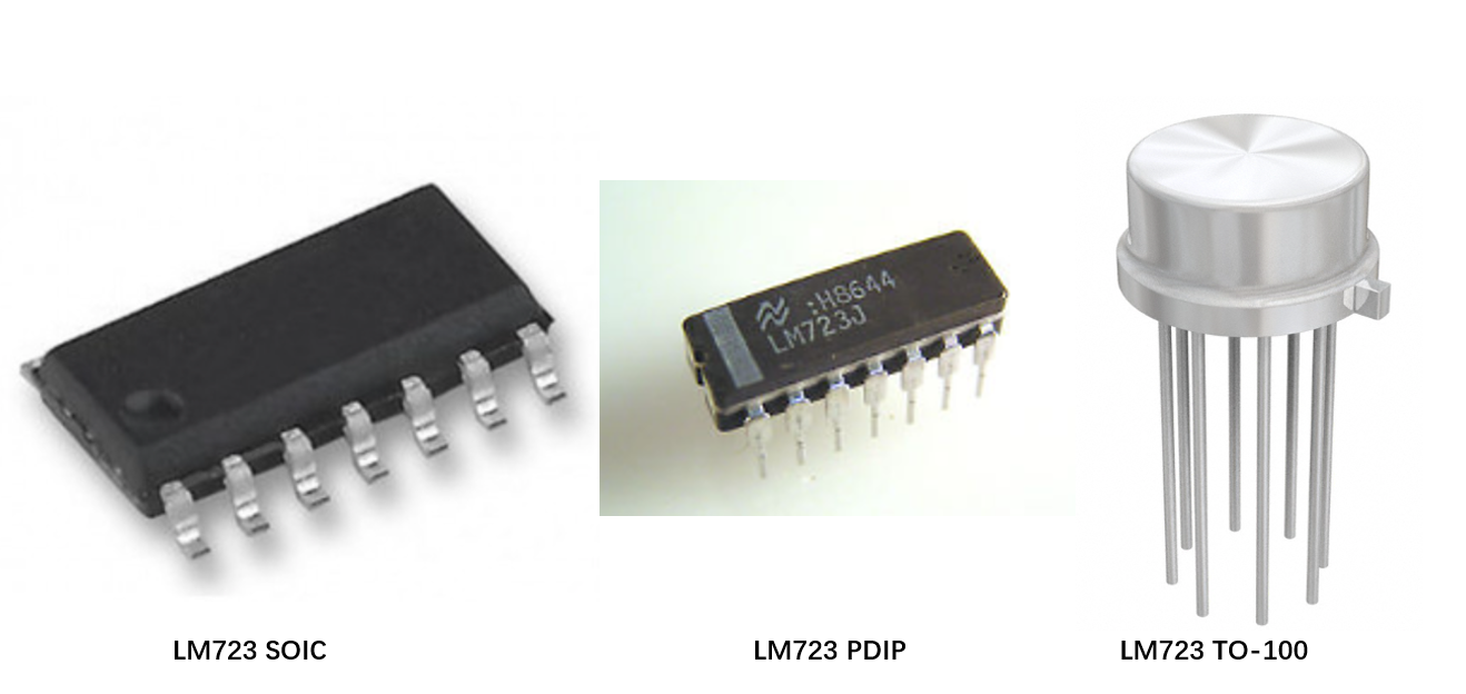
LM723 Typical Packages
LM723 is available in several packages due to its high demand and extensive use in various analog and power electronics applications. The most common packages of LM723 are PDIP, SOIC, and TO-100. The electrical characteristics of all the LM723 packages are identical; the difference lies only in form factor, thermal characteristics, and mounting style. Different packages type has different unique packaging codes, making it easier for the customer to buy the exact LM723 IC.
LM723 Package Details
Different LM723 package options and their characteristics.
| Package Type | Package Code | Description |
|---|---|---|
| DIP-14 (Dual in Line Package) | LM723CN | Most common version; ideal for through-hole circuits and educational setups. |
| TO-100 Metal Can Package | LM723H | Offers better thermal stability and EMI resistance for industrial applications. |
| SOIC-14 (Surface Mount) | LM723MD | Compact SMD version for modern PCB layouts and automated assembly. |
Choose the LM723 package type based on your circuit design and assembly method.
LM723 Internal Circuit & Working Operation
LM723 is a monolithic integrated programmable voltage regulator, assembled in a 14-lead dual-in-line plastic package. Unlike 7805 and 7812 voltage regulators that only provide fix output voltage, LM723 offers adjustable voltage regulation and 150mA output current.
LM723 generates the adjustable voltage by comparing its output voltage to a stable internal reference voltage. LM723 consists of an error amplifier that adjusts a series pass transistor to maintain a constant output voltage, irrespective of changes in the input supply voltage.
The internal circuit of LM723 consists of several key circuits that together make the working operation of LM723 precise and accurate. Key internal circuit components are the voltage reference circuit, error amplifier, series pass transistor, current limiting circuit, and frequency compensation circuit.
Voltage Reference Circuit
The internal circuit consists of a zener diode and a buffer circuit that provides a highly stable reference voltage. This voltage is 7.15 volts and appears on Vref (PIN 6).
Error Amplifier
The output of the reference voltage circuit, i.e., 7.15 volts, is given to the high-gain differential amplifier known as the error amplifier. The reference voltage is given to pin 5, which is the non-inverting input of the amplifier, and its inverting input (Pin 4) receives a feedback voltage from the regulated output.
Series Pass Transistor
The output of the error amplifier is responsible for driving the NPN pass transistor. Pin 11 of the LM723 is connected to the unregulated input supply, and the emitter provides the output voltage at pin 10 (Vout).
Current Limiting Circuit
A separate internal NPN transistor is used for current protection. Its base and emitter are connected to the Current Limit (CL, Pin 2) and Current Sense (CS, Pin 3) pins, respectively. When the voltage drop across an external current-sensing resistor (connected between CL and CS) exceeds approximately 0.65V, this transistor turns on and limits the drive to the main pass transistor, thereby limiting the output current.
Frequency Compensation
An external capacitor (typically 100 pF) is connected between the Frequency Compensation pin (Pin 13) and the inverting input (Pin 4) to prevent the error amplifier from oscillating.
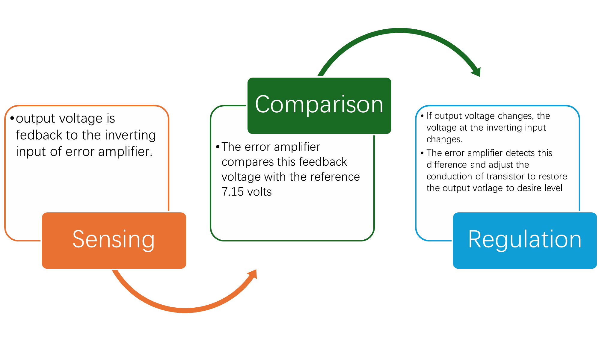
Working Operation of LM723
Sensing
A portion of the output voltage is fed back to the inverting input of the internal error amplifier via an external resistor network (usually a potentiometer for an adjustable output).
Comparison
The error amplifier compares this feedback voltage with the stable 7.15V internal reference voltage applied to its non-inverting input.
Regulation
If the output voltage changes (e.g., drops due to increased load), the voltage at the inverting input changes. The error amplifier detects this difference and adjusts the conduction of the series pass transistor to restore the output voltage to the desired level.
Electrical Characteristics & Technical Specifications
When searching for the LM723 voltage regulator datasheet or LM723 part number, one of the most crucial sections engineers look for is its electrical characteristics and technical specifications. LM723 is a versatile and extensively use adjustable voltage regulator that is a popular choice for many engineers to utilize in their circuit applications.
However, understanding its electrical and technical specifications is essential for engineers to use it in their design applications effectively. Different variants of LM723 are also available, such as LM723C; therefore, it is important to consult the datasheet for the exact and accurate technical specifications.
LM723 Technical Specifications (Absolute Maximum Ratings)
Key absolute maximum ratings and limits.
| Parameter | Max Value | Description |
|---|---|---|
| Supply Voltage | 40V | Maximum input voltage across the IC |
| Output Current (without pass transistor) | 150mA | Internal transistor current limit |
| Reference Voltage | 7.15V | Stable internal voltage reference |
| Output Voltage Range | 2 – 37V | Adjustable via external resistors |
| Power Dissipation | 660 mW | The maximum power that can be safely dissipated |
| Operating Junction Temperature Range | 0°C to +125°C | Suitable for industrial and lab applications |
| Storage Temperature Range | -65°C to +150°C | Safe storage range without degradation |
Always confirm values with the official LM723 datasheet before use.
LM723 Electrical Characteristics (Typical Performance)
Representative electrical performance parameters of the LM723 voltage regulator.
| Parameter | Typical Value |
|---|---|
| Reference Voltage | 7.15V |
| Short Circuit Current Limit | 10 – 150mA |
| Input Bias Current (Error Amplifier) | 100nA |
| Ripple Rejection Ratio | 74dB |
| Output Noise Voltage | 86 µV rms |
| Dropout Voltage | 3V |
Typical values are measured under standard test conditions; consult the datasheet for guaranteed limits.
Design Guide and Calculations
Designing a stable and efficient LM723 voltage regulator circuit requires understanding the IC’s internal structure, pin functions, and external components that determine its output voltage, current limit, and stability.
The LM723 is one of the most versatile linear voltage regulators, capable of operating as a low-voltage regulator (2 V–7 V) or high-voltage regulator (up to 37 V), and even supporting external pass transistors for higher current applications.
This section serves as a complete LM723 design guide—covering pin-level wiring, external component design, calculation formulas, and a worked example that integrates all these principles into a real-world circuit.
Step-by-Step Wiring Guide of LM723
LM723 Connection Guide
1. Connect V+ (pin 12) to the unregulated input supply (e.g., 12 V).
2. V− (pin 7) to ground.
3. Use a 0.1 µF ceramic bypass capacitor close to the IC between pins 12 and 7.
4. Also, Connect pin 6 (Vref) to one leg of a resistor divider (R1–R2) used for output voltage adjustment.
5. Feedback from the output node goes to +IN (pin 5) via the divider network.
6. Tie −IN (pin 4) to the reference node (either ground or Vref, depending on configuration).
7. Add a Cref ≈ 5 µF between pin 6 and ground to improve ripple rejection.
💡 Tip: Keep wiring short and use proper decoupling for best regulator stability.
External Circuit Design Guidelines
Voltage Divider Network (R1–R2):
The LM723’s output voltage is controlled by comparing a portion of Vout to its internal 7.15 V reference. For series regulator configuration;
Where Vref is 7.15V and use $R_1 = 1\,\text{k}\Omega \text{–} 10\,\text{k}\Omega$ for a stable bias current and choose R2 to set the desired output.
External Pass Transistor (High-Current Applications):
The internal transistor of LM723 can deliver ~150 mA. For higher current, connect an NPN pass transistor such as 2N3055:
Transistor Connections
- 1
Collector → VIN (raw supply)
- 2
Emitter → Load / VOUT terminal
- 3
Base → Pin 10 (VOUT) through 100 Ω resistor.
Tip: place the base resistor close to the transistor base and keep wiring short for stable operation.
The LM723 then drives the external transistor base to maintain a regulated output voltage.
Current Limit Design:
Place a low-value resistor (Rsc) between internal VOUT (pin 10) and the regulated output node.
Connect pin 2 (CL) and pin 3 (CS) across this resistor.
LM723 Current Limit Equation
💡 Adjust Rsc (sense resistor) to set the desired current limit.
For instance, to achieve 1A current, place a resistor of 0.65Ω. For foldback current limiting, add a resistor network between pins 2, 3, and 4.
Compensation & Stability:
Connect a 100 pF–1 nF capacitor from pin 13 (Comp) to ground to prevent oscillation.
Use a 5 µF capacitor from Vref (pin 6) to ground for high ripple rejection.
Add an electrolytic capacitor (10–470 µF) at the output to minimize ripple.
Thermal & Dropout Considerations:
Ensure $V_{IN} \ge V_{OUT} + 3\,\text{V}$ to maintain regulation.
External transistor dissipation $P \approx (V_{IN} – V_{OUT}) \times I_{OUT}$ ; Always mount it on a heatsink.
Practical Design Example
Regulated 12 V / 1 A DC Power Supply Design
Using LM723 voltage regulator with an external pass transistor
To compute the output voltage, the external resistor divider network R1 and R2 across the Vref (pin 6) and non-inverting input terminal (pin 5) needs to be determined. The formula to calculate the Vout of LM723 is;
If I choose R1 to be 2.2KΩ, and Vref is 7.15V and Vout is 12V, then R2 will become;
Voltage Divider Calculation for LM723
Therefore, to maintain a 12V output voltage, the value of R2 should be $R_1 = 3.2\,\text{k}\Omega$ and R1 is $R_2 = 2.2\,\text{k}\Omega$
To deliver the 1A current at the output of LM723, use an external pass transistor (2N3055 NPN transistor). Connect the collector of the transistor with an 18V input, the base with pin 10 via a $100\,\text{k}\Omega$ resistor, and the emitter terminal with a 12V output.
For 1A output current, place a 0.65Ω resistor between pin 10 of LM723 and base of the transistor.
Current Sense Resistor Calculation
Used to limit the load current to 1 A in the LM723 regulated supply design.
For stability and noise reduction, connect the following capacitors.
LM723 Capacitor Connections
- CIN: 0.1 µF + 470 µF at input
- COUT: 470 µF at output
- CREF: 5 µF at pin 6 to ground
- CCOMP: 100 pF at pin 13 to ground
LM723 Practical PCB Layout Considerations
70% of LM723-based regulator failures are caused not by circuit design errors, but by bad PCB layout. Let’s make sure yours isn’t one of them.
Designing a voltage regulator with the LM723 IC is more than just connecting pins and resistors; the printed circuit board (PCB) layout directly affects voltage stability, ripple, and noise rejection. A poor layout can cause oscillations, thermal drift, or even failure of the pass transistor. In this section, we will explore some of the best and key PCB layout considerations to make your LM723 voltage regulator on PCB work perfectly without any errors or failures.
Component Placement Strategy
Proper component placement is the first step to a clean and stable design.
-Place the LM723 IC close to the input and output filter capacitors to reduce lead inductance.
-The reference bypass capacitor (0.1 µF) between Vref (Pin 6) and GND (Pin 7) should be placed as close as physically possible to the IC pins.
-Keep R1 and R2 (feedback resistors) close to the IC to avoid noise pickup on the feedback line.
-The sense resistor (Rsense) for current limiting must be placed directly in the load return path and connected with thick traces.
Grounding Techniques
Grounding mistakes are one of the biggest noise sources in LM723 circuits and overall in PCB designs. To minimize the noise from grounding, follow these guidelines.
-Never mix a high-current load ground with a signal ground directly.
-Connect the LM723’s GND (Pin 7) and Vref bypass capacitor to a quiet signal ground branch.
-The output stage ground (Rsense, load return) should go to a separate high-current trace that joins at the main ground point.
LM723 Typical Circuit Applications
Whether you need a 5V precision reference, a 30V lab bench supply, or a constant current charger, LM723 can do it all with just a few external components. Visit the video below which explains a step-by-step design guide for the solar charge controller circuit application using LM723.
If you’re designing a DC power supply, high-current regulator, or a negative voltage source, the LM723 Voltage Regulator IC offers unmatched versatility. Its ability to work across wide voltage and current ranges makes it a favorite among engineers and hobbyists alike. In this section, we’ll explore three practical LM723 application circuits, each with complete wiring explanation, working principle, and step-by-step connection guide.
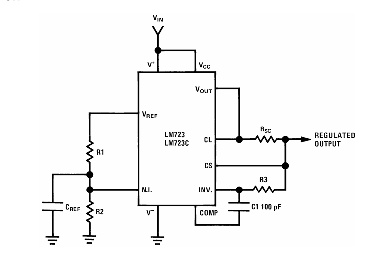
Basic High Voltage Regulator (07-37 Volts)
This is the standard LM723 voltage regulator circuit, capable of regulating outputs between 7V and 37V. It uses the internal reference (Vref) and error amplifier to maintain a stable DC output.
The LM723 senses the difference between the reference voltage (7.15V) and the feedback voltage from the resistor divider. The internal amplifier adjusts the output drive to maintain the desired regulated voltage at the output.

The output of this LM723 voltage regulated using the following formula
LM723 Circuit Connection Guide
- VCC (Pin 12): Connect to input supply (VIN).
- Vref (Pin 6): Provides a stable 7.15V internal reference.
- Non-Inverting Input (Pin 5): Receives feedback voltage from the divider network (R1 and R2).
- Inverting Input (Pin 4): Compares feedback voltage with reference.
- Output (Pin 10): Provides regulated output voltage.
- RSC (Current Sense Resistor): Limits output current.
- C1 (100 pF): Stabilizes loop gain to prevent oscillation.
Negative Voltage Regulator
This configuration allows the LM723 to regulate negative output voltages, ideal for dual power supply systems (e.g., ±12V or ±15V for op-amp circuits). It cleverly reverses the supply and ground reference to generate a negative output.
The LM723 maintains a fixed potential difference between its reference and output terminals. Since the ground reference is inverted, the regulator effectively generates a negative regulated output.
LM723 Circuit Connection Guide (Negative Input Configuration)
- V+ (Pin 12): Connected to ground in this configuration.
- V− (Pin 7): Connected to negative input voltage.
- Vref (Pin 6): Still provides +7.15 V reference internally.
- R3–R4 Network: Defines the output voltage level.
- C1 (100 pF): Maintains phase stability.
- Output: Taken from the emitter of the pass transistor or from the IC’s output pin.
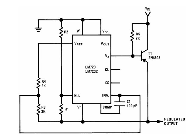
Positive Voltage Regulator with External Pass Transistor for High Output Current
When higher output current is needed beyond the LM723’s internal limit (≈150 mA), an external pass transistor like 2N3054 or 2N3771 is added. This configuration allows the LM723 to handle currents up to 10A or more, depending on transistor capability and heat dissipation.
The LM723 controls the base of the transistor (T1). As load current increases, the transistor supplies additional current, keeping the output stable. The internal amplifier modulates T1’s conduction to maintain the desired voltage across the load.

LM723 + External Pass Transistor Connection Guide
- T1 (2N3054): Functions as the external series pass transistor.
- Base of T1: Driven by the LM723’s output (Pin 10).
- Emitter of T1: Provides the regulated output.
- RSC: Senses output current for protection.
- R1–R2: Voltage divider network sets output voltage.
- C1 (500 pF): Ensures compensation and loop stability.
Advantages & Limitations of LM723 Voltage Regulator
Advantages & Limitations of LM723
| Advantages of LM723 | Limitations of LM723 |
|---|---|
| Wide Output Voltage Range: Can regulate voltages from 2 V to 37 V, suitable for diverse applications. | Maximum Output Voltage Limitation: Cannot directly regulate above 37 V without external circuitry. |
| Adjustable & Fixed Voltage: Supports adjustable voltage via resistors and fixed voltage configurations. | External Components Required for High Current: Output above 150 mA needs external pass transistors. |
| High Output Current Capability: Can supply up to 10 A with an external pass transistor. | Not Suitable for High-Frequency Switching: Being linear, it dissipates excess voltage as heat. |
| Internal Precision Reference: Built-in 7.15 V reference ensures accurate voltage regulation. | Moderate Load & Line Regulation: Less precise compared to modern LDOs or switching ICs. |
| Short-Circuit & Thermal Protection: Includes internal current limiting and thermal shutdown. | Less Integration: Requires external components for features available in modern ICs. |
| Low Dropout Voltage (with external transistor): Improves efficiency in battery-powered circuits. | Thermal Management Required: High currents produce heat, needing heat sinks. |
| Cost-Effective & Reliable: Widely available and affordable for hobbyists and industrial projects. | NA |
LM723 VS Alternatives
The LM723 voltage regulator IC is a classic choice for linear voltage regulation. However, with modern alternatives available, it’s essential to understand the differences, advantages, and ideal applications of LM723 compared to other voltage regulators like LM317, 7805, LM338, and modern LDOs.

Conclusion
The LM723 voltage regulator IC remains a versatile and reliable choice for linear power supply designs, offering a combination of adjustable output, built-in reference voltage, and protection features. Its ability to support medium to high output currents with external pass transistors, along with short-circuit and thermal protection, makes it suitable for a wide range of applications, including bench power supplies, audio amplifiers, and industrial circuits.
Frequently Asked Questions (FAQ)
Use external series pass transistors like 2N3055 or TIP3055. Ensure proper base resistor calculation and adequate heat sinking for both the IC and transistor to handle currents up to 10 A safely.
Yes, LM723 can be configured to regulate positive or negative voltages by adjusting the circuit topology, making it suitable for dual power supplies in op-amp circuits or audio amplifiers.
The output voltage is set by the resistor network connected to the non-inverting input and Vref. Use high-precision resistors (1% or better) and calculate according to the Vout formula mention in the design guide section.
Absolutely. Its adjustable output and protection features make it perfect for DIY lab power supplies, allowing precise voltage control and current limiting.
The IC reduces output current or shuts down when overheated or overloaded. This protects components but may limit output under high load. Always design with adequate heat sinking and current rating to avoid frequent triggering.
You can improve regulation by:
-Using low-value precision resistors in the voltage divider
-Adding a high-gain external transistor for the pass element
-Minimizing wiring resistance and stray inductance in high-current paths