Introduction
Modern electronic devices are voltage sensitive and require efficient power regulation. Switch mode power regulation is becoming popular due to its minimum heat generation and its light weight. The TL494 device is the complete package that contains all the circuitry in a single IC to generate the Pulse Width Modulation (PWM). This chip generates the Pulse Width Modulation (PWM) that switches ON/OFF the external transistor in Switch Mode Power Supplies (SMPS). Apart from the SMPS, the TL494 PWM controller is widely use in various application circuits, including Personal Computers (PCs), microwave ovens, Solar power inverters, and smoke detectors.
TL494 is a versatile fixed frequency PWM controller that consists of a 5V reference regulator, an Oscillator circuit, a dead time control circuit, a voltage comparator circuit , a PWM circuit, error amplifiers, and an output control circuit. In this article, I will comprehensively explain the working operation of the TL494 PWM controller and explain each part of it. Upon completion of this article, you will be able to understand the TL494 pinout, its working operation, circuit design parameters, and software simulations to gain practical insight into TL494.
What is the TL494 PWM Controller?
The TL494 is a 16-pin fixed frequency Pulse Width Modulation (PWM) controller IC that is mainly use in Switch Mode Power Supplies, i.e., DC-DC converters such as buck and boost converters. TL494 generates the control PWM that is useful in many more applications, including battery chargers, inverters, servers, and Power Supply Units (PSUs). The TL494 PWM controller contains built-in two error amplifiers, an on-chip adjustable oscillator, a dead time control comparator, a pulse steering control flip flop, and a 5V precision regulator. dead time. These unique features make the TL494 PWM controller a perfect choice for engineers, hobbyists, and professionals.
The TL494 generates the PWM at the output terminal by comparing a fixed-frequency sawtooth waveform with the voltage produced by two error amplifiers. The comprehensive working operation will be discussed later in this article.
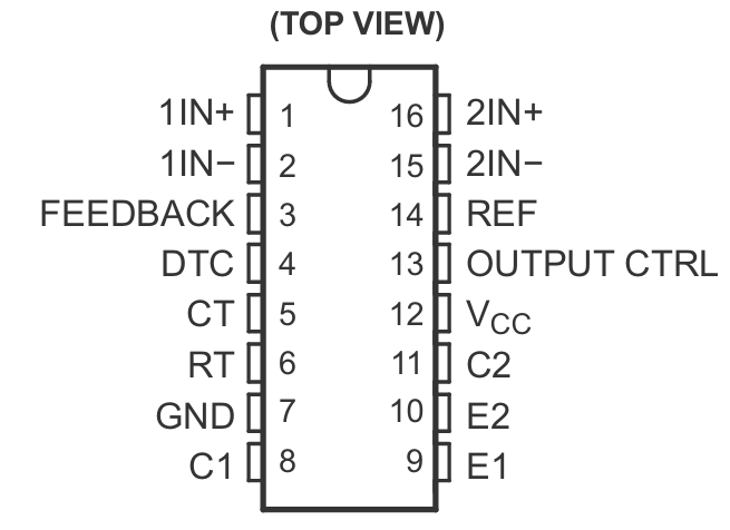
TL494 PIN Configuration
TL494 PWM controller is a 16-pin IC that mostly comes in SOIC, SOP, and TSSOP packages. This popular PWM controller is designed and manufacture by Texas Instruments.
TL494 PIN Configuration
| PIN Number | PIN Name | Function |
|---|---|---|
| 1 | 1-IN+ | This is the non-inverting input of error amplifier 1 |
| 2 | 1-IN- | Inverting the input of error amplifier 1 |
| 3 | Feedback | Feedback input of error amplifier 1 |
| 4 | DTC | Dead Time Control comparator input |
| 5 | CT | This pin is used to set the oscillator frequency using the capacitor terminal |
| 6 | RT | This pin is used to set the oscillator frequency using the resistor terminal |
| 7 | GND | Common Ground of the circuit |
| 8 | C1 | Collector terminal output of BJT 1 |
| 9 | E1 | Emitter terminal output of BJT 1 |
| 10 | E2 | Emitter terminal output of BJT 2 |
| 11 | C2 | Collector terminal output of BJT 2 |
| 12 | VCC | Positive supply of TL494 (7V–40V) |
| 13 | OUTPUT CTRL | This pin decides the push-pull or single-ended operation of the IC |
| 14 | REF | This pin gives the reference 5V regulator output |
| 15 | 2-IN- | Inverting the input of error amplifier 2 |
| 16 | 2-IN+ | This is the non-inverting input of error amplifier 2 |
Printed Circuit Board Design Considerations
In circuit board design, when the surface mount package is used, it is recommended to use a well-regulated input supply and keep it within a few inches from the device. However, if it is not the case, then we must use tantalum capacitor with a value of 47uF. Try to make the power track thick and short.
The feedback traces of error amplifiers should be far away from the power tracks and noisy tracks. Also, try to make the feedback traces direct and thick. Always place the input ceramic capacitor close to the VCC pin. This will eliminate the noise and inductance effects and provide a clean voltage to the VCC pin. Other external components of the TL494 IC should be placed close to the IC to eliminate the noise and avoid signal loss.

TL494 Circuit and Working Operation
The internal circuit of TL494 consists of various sub-circuits that together generate the required PWM. In this section, I will explain the working operation of the TL494 PWM controller. The PWM controller IC’s internal circuit consists of an oscillator circuit, a dead time comparator, two error amplifiers, a PWM comparator, and an output circuit. Each circuit within the TL494 has its own function.
Oscillator Circuit and Error Amplifiers
The TL494 generates the PWM signals at the output by comparing the sawtooth signal with the reference voltage of 5V. An oscillator circuit generates the sawtooth waveform by using the external timing resistor (RT) and timing Capacitor (CT). The output of this oscillator circuit produces the sawtooth waveform. The two error amplifier circuits are used to compare the feedback of the supply output (actual output) with the reference 5V. The difference between the actual and the desired output is the error signal. This error signal determines the duty cycle of TL494.
PWM Comparator
The resultant error signal is now use as an input to the comparator circuit. This PWM comparator circuit compares the error signal with the sawtooth waveform, which is generated from the oscillator circuit. When the error signal is higher than the sawtooth signal, the PWM comparator turns ON the BJT, resulting in an ON PWM pulse. However, when the error voltage is less than the sawtooth ramp, the PWM comparator turn OFF the BJT, results in OFF PWM pulse. This process creates a PWM signal and ensures power regulation is smooth.
Dead Time Control Circuit
The TL494 circuitry includes the protection circuit known as the dead time control circuit. The purpose of this circuit is to ensure that the output BJT transistors should never ON at the same time. This is important because keeping both transistors ON at any time will cause the short circuit and excess flow of current will damage the IC.
Output Circuit
This is the output of TL494, and this circuit decides whether to use it in push-pull configuration or single-ended output. If TL494 is configured as single-ended, only one transistor is used. However, if you configure the TL494 in push-pull configuration, both transistors will operate but independently.
Technical Specifications & Parameters
TL494 is a powerful PWM controller that integrates oscillator circuit, PWM comparator circuit, and error amplifier circuit into one single package, resulting in an efficient and reliable product for a range of electronic applications such as inverters, battery charging, and DC-DC converters. The TL494 internal circuit is complex and requires a comprehensive understanding of the IC operation and its technical specifications and parameters. The key technical specifications and parameters of TL494 help the designer to use it in their design with efficiency and accuracy. For more technical specifications and parameters of TL494, please take a look at the datasheet from Texas Instruments.
TL494 Technical Specifications & Parameters
| Parameter | Value | Function |
|---|---|---|
| Operating voltage range (VCC) | 7–42 Volts | This ensures the stable operation of the PWM controller in both low and high SMPS applications. |
| Reference voltage | 5V | TL494 internally provides a 5V reference voltage for feedback |
| Oscillator frequency range | 1kHz to 300kHz | The external timing resistor (RT) and timing capacitor (CT) determine the oscillator frequency. |
| Dead time control range | 0%–100% | This is an adjustable delay to avoid transistor overlap |
| Output transistor saturation voltage | 1.3 V typical | This is the output saturation voltage in common emitter configuration. |
| Operating junction temperature | –40°C to +85°C | This is the TL494 normal operating temperature range. |
Circuit Design with TL494 PWM controller
To use TL494 in your circuit design you must have first know your design requirements. Secondly, you must have the TL494 design parameters and specification knowledge which you can see from the datasheet. Thirdly, you must have the knowledge of typical application circuit of TL494 so that you can use it in your design. In this section, I will use an example to explain the design calculations and TL494 configuration. The same procedure you may follow to calculate and configure TL494 as per your requirement.
Design Example: Buck Converter using TL494 (Requirements)
|
Oscillator Frequency Calculation
The very first step in designing with TL494 is the calculation of oscillator frequency. The oscillator frequency generates the sawtooth waveform that is use as in PWM comparator circuit for comparison. The oscillator frequency is programmed using the one external timing resistor (RT), and one timing capacitor (CT). The values of RT and CT determine the oscillator frequency of the TL494. The formula to determine the oscillator frequency according to the TL494 datasheet is as follows;
\[ f_{osc} = \frac{1}{R_T \times C_T} \]
The above formula is use to calculate the oscillator frequency of TL494 for single ended applications only. For push-pull applications the formula to calculate the oscillator frequency is as follows;
\[ f_{osc} = \frac{1}{2 \times (R_T \times C_T)} \]
From the above formula for push-pull applications, it is clear that the output frequency in push pull applications is one half of the oscillator frequency.
Our design requirement is to operate the TL494 at 20kHz switching frequency and for single ended application. If we choose a standard CT value of 0.001uF than we can find the value of timing resistor RT for 20KHz PWM operation.
\[
f_{osc} = \frac{1}{R_T \times C_T}
\]
\[
20,000 = \frac{1}{R_T \times 0.001 \,\mu F}
\]
\[
R_T = \frac{1}{20,000 \times 0.001 \,\mu F}
\]
\[
R_T = 50 \, k\Omega
\]
Error Amplifiers and Feedback Configuration
The internal circuit of TL494 consist of a 5V voltage reference that is divided into 2.5V using the R3 and R4 resistors. The output signal error is also divided to 2.5V using the R8 and R9 as shown in the circuit diagram. To make the adjustment of output voltage at exactly 5V, a potentiometer of 10kΩ can also be use for exact 5V regulated output.
To make the 5V reference to 2.5 the resistor values of R3 and R4 should be 5.1KΩ.
\[
V_{out} = V_{in} \cdot \frac{R_4}{R_3 + R_4}
\]
\[
V_{out} = 5V \cdot \frac{5.1}{5.1 + 5.1}
\]
\[
V_{output} = 2.5V
\]
Dead Time Control (DTC) Configuration
A big surge at the start occurs on the switching transistors. To reduce the stress the charging of filter capacitor must be reduced. The soft start allows the PWM to increase slowly and prevent the initial surge. This is achieve by using the negative slope waveform using the R7 and C2 at PIN 4. The capacitor charges through resistor R6, resulting in slow initial increase in output PWM.
Typically, a soft start means 25-50 clock cycles. If we choose 50 cycles for a soft start for our design problem.
\[
t = \frac{1}{f}
\]
\[
t = \frac{1}{20\,kHz} = 50\,\mu s
\]
It is therefore, the capacitor \(C_2\) value should be:
\[
C_2 = \frac{\text{Soft start time} \times 50 \, \text{cycles}}{R_6}
\]
\[
C_2 = \frac{50\mu s \times 50}{1k\Omega}
\]
This value of capacitor will ensure to prevent any false signals.
\[
C_2 = 2.5\mu F
\]
Buck Converter Filter Inductor Calculations
For the buck converter design one important component is the inductor and accurately calculating its value as per the design requirements. For the buck converter for an input voltage of 32V and output voltage of 5V. The duty cycle of buck converter is;
\[
D = \frac{V_o}{V_i}
\]
\[
D = \frac{5}{32} = 0.156
\]
\[
\text{Switching frequency } (f) = 20 \, kHz
\]
\[
t_{on} = \frac{1}{f} \times D = 0.00005 \times 0.156 = 7.8 \, \mu s
\quad (\text{when switch is closed})
\]
\[
t_{off} = \frac{1}{f} – t_{on} = 0.00005 – 7.8 \, \mu s = 42.2 \, \mu s
\quad (\text{when switch is open})
\]
Using the theoretical derivations of buck converter design parameters found in literature, the value of inductor (L) is found out using the formula;
\[
L = \frac{V_i – V_o}{t_{on} \times \Delta I_L}
\]
Where ΔIL is given in the design requirements. Therefore, the inductor value will be;
\[
L = \frac{32 – 5}{7.8\mu s \times 1.5A}
\]
\[
L = 140.4 \, \mu H
\]
Buck Converter Filter Capacitor Calculations
Another design component of buck converter is the filter capacitor. Accurately calculating its value is important because it filter out the voltage ripples at the output of buck converter. The filter inductor eliminates the currents ripples at the output of buck converter and filter capacitor eliminates the voltage ripples at the output.
The maximum peak to peak allowable ripple voltage is given in the design requirement i.e. 20mV peak to peak. By using the ripple voltage, we can find the effective series resistance according to the formula;
\[
\text{Effective Series Resistance (ESR)} = \frac{V_R}{\Delta I_L}
\]
\[
ESR = \frac{20mV}{1.5A} = 0.067 \, \Omega
\]
From the ESR, we can find the minimum capacitance require to maintain the peak-to-peak ripple below 100mV using the formula;
\[
C = \frac{\Delta I_L}{8 f V_R} \\
C = \frac{1.5\text{ A}}{8 \cdot 20\,\text{kHz} \cdot 0.1\text{ V}} \\
C \approx 94\,\mu\text{F}
\]
Output Stage Configuration
The PWM controller TL494 has two output transistors to generate the output PWM. The collector of transistors is connected with pin 8 and 11. The emitters of both transistors are connected with PIN 9 and 10. The TL494 can be configure as single ended mode or push pull mode.
Common Circuit Applications with TL494 PWM Controller
TL494 is a powerful PWM controller that is widely use in various power electronic applications including inverter design, battery charging, and DC-DC converters such as buck and boost converter. In this section, I will explain some of the most common applications circuit of TL494 PWM controller using the practical software demonstration and results.
Basic PWM generation using the TL494 IC
In this example, I have use Proteus software to simulate the TL494 to generate the PWM signals. SMPS, inverter circuits, and battery charging circuits require continuous PWM signals to Turn ON/OFF the transistor switches. By changing the duty cycle the average voltage across the output of the circuit is changing as shown in the circuit diagram.
To generate the PWM signals using the TL494, we need to configure the TL494 such as oscillator frequency calculation using the RT resistor and CT capacitor. This generates the sawtooth waveforms for comparison with PWM comparator circuit. The oscillator frequency for this particular circuit is set using the 100KΩ RT resistor and 100nF CT capacitor. For the single ended operation, we connect the PIN 13 (CTRL) pin to GND.
The TL494 has two output transistor and are open collector outputs. So, two pull up resistors and two external BC547 transistors are used. The purpose of these external transistors is to amplify the output signals such that they are strong enough to drive the load. The PWM signals at the output as shown in the output waveforms in figure below can be use for any low power switching applications. We connect the DTC pin with GND because there is no need of dead time control in this circuit.


For hardware implementation of PWM inverter circuit step by step guide, visit this “PWM inverter circuit using TL494“.
Buck Converter using TL494
Buck converter circuit is the type of DC-DC converter that step down the input voltage. Unlike the voltage regulator circuit, the DC-DC converter uses the Pulse Width Modulation technique to step down the input voltage. In the circuit design with TL494 section, we have calculated the different values of buck converter circuit including the oscillator frequency, error amplifier configuration, filter inductor value, filer capacitor value, and output transistor stage configuration. All these values are reflected in the above circuit of buck converter using TL494.

Simulation Results: Speed Control of Motor using TL494
The TL494 PWM controller IC can also be use to drive the motor and control its speed. The speed of the motor can be control by varying the duty cycle. In this circuit I have use TL494 and two MOSFET circuits to control the speed of motor as shown in figure below. The oscillator frequency which determines the PWM of TL494 is set using the RT and CT (PIN 5 and PIN6).
\[ f_{osc} = \frac{1}{R_T \times C_T} \]
The values of RT and CT are 10k and 1uF respectively.
To control the duty cycle of the output PWM signals, a variable resistor RV1 is use; by changing the resistance of RV1, we can control the speed of motor. This variable RV1 is applied at the input of non-inverting input of TL494. When the RV1 changes the voltage also changes and thus setting the motor speed reference. To sense the motor current, a shunt resistor is use with transistor Q3 as shown in circuit diagram. To prevent the both IRF1010 MOSFETs to TURN ON simultaneously, dead time control pin is an RC network is use at the PIN 4 of TL494. The capacitor C1 and C2 acts as the filter capacitor to remove the ripples voltages. The motor is connected across the load and upon varying the duty cycle the speed of motor can be also be observed.

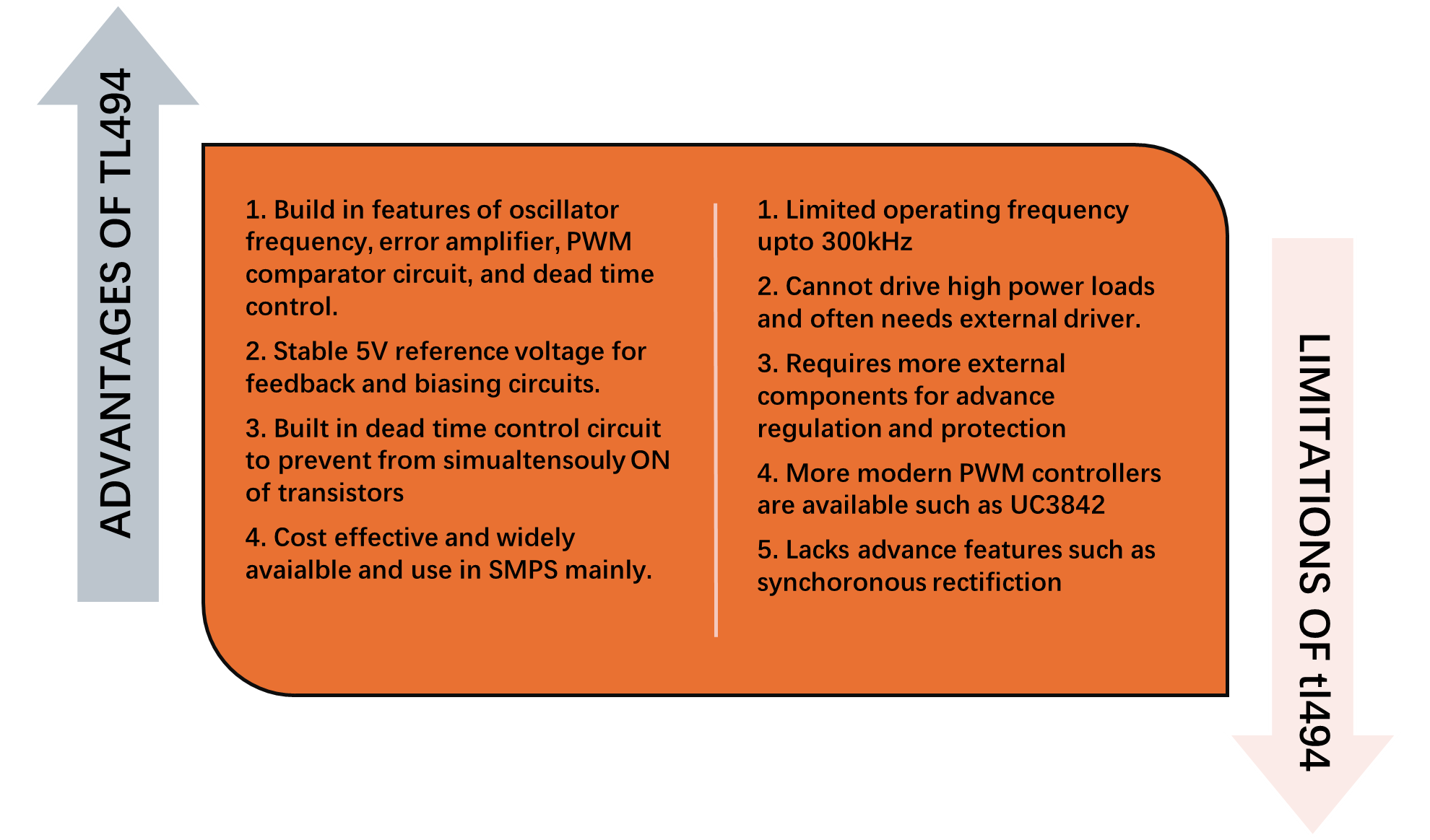
Advantages and Limitations of TL494
TL494 is a verstile and powerful PWM controller chip but like every device it does have its own advanatages and limitations.
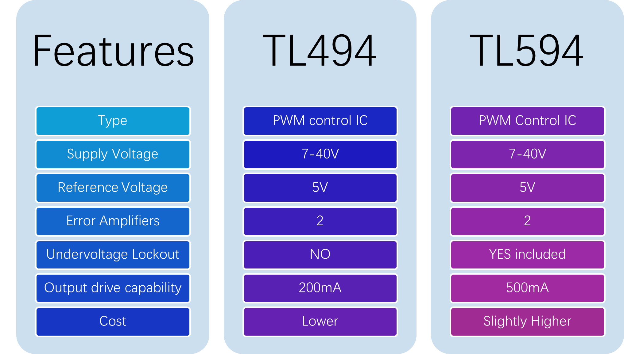
TL494 VS TL594
Conclusion
The TL494 PWM controller is the versatile device that is widely use in power electronic applications including motor drive speed controller, inverter circuits, solar inverter circuits, microwave ovens, smoke detectors, battery charging circuits, and switch mode power supplies. Understanding the working operation of TL494, its pinout, and circuit design is important for power electronic engineers to efficiently utilize its capabilities into their designs.
Frequently Asked Questions (FAQ)
Q1. What is TL494 IC use for?
TL494 is the PWM controller IC that is widely use in power electronic applications including SMPS, solar inverter circuits, battery charging circuits, and motor speed control applications.
Q2. What is the difference between TL494 and TL594
TL594 is the up version of TL494. Both are PWM controller except for the fact that TL594 has more current capability and some extra protection built in features.
Q3. How does the TL494 control the output voltage?
The internal circuit of TL495 consist of oscillator circuit that generates the sawtooth waveform, and error amplifier circuit that compare the feedback signal with 5V reference voltage. Therefore, by adjusting the voltage the TL494 control its output voltage.
Q4. Can I use TL494 for motor control application?
Yes, TL494 is use in motor control applications. By adjusting the duty cycle the speed of motor can be controlled.
Q5. What is the output current capability of TL494
The maximum output current capability of TL494 is 200mA.
Q6. What are some alternatives to TL494
You can use TL594, SG3524, and UC3842 depending on the application requirements.