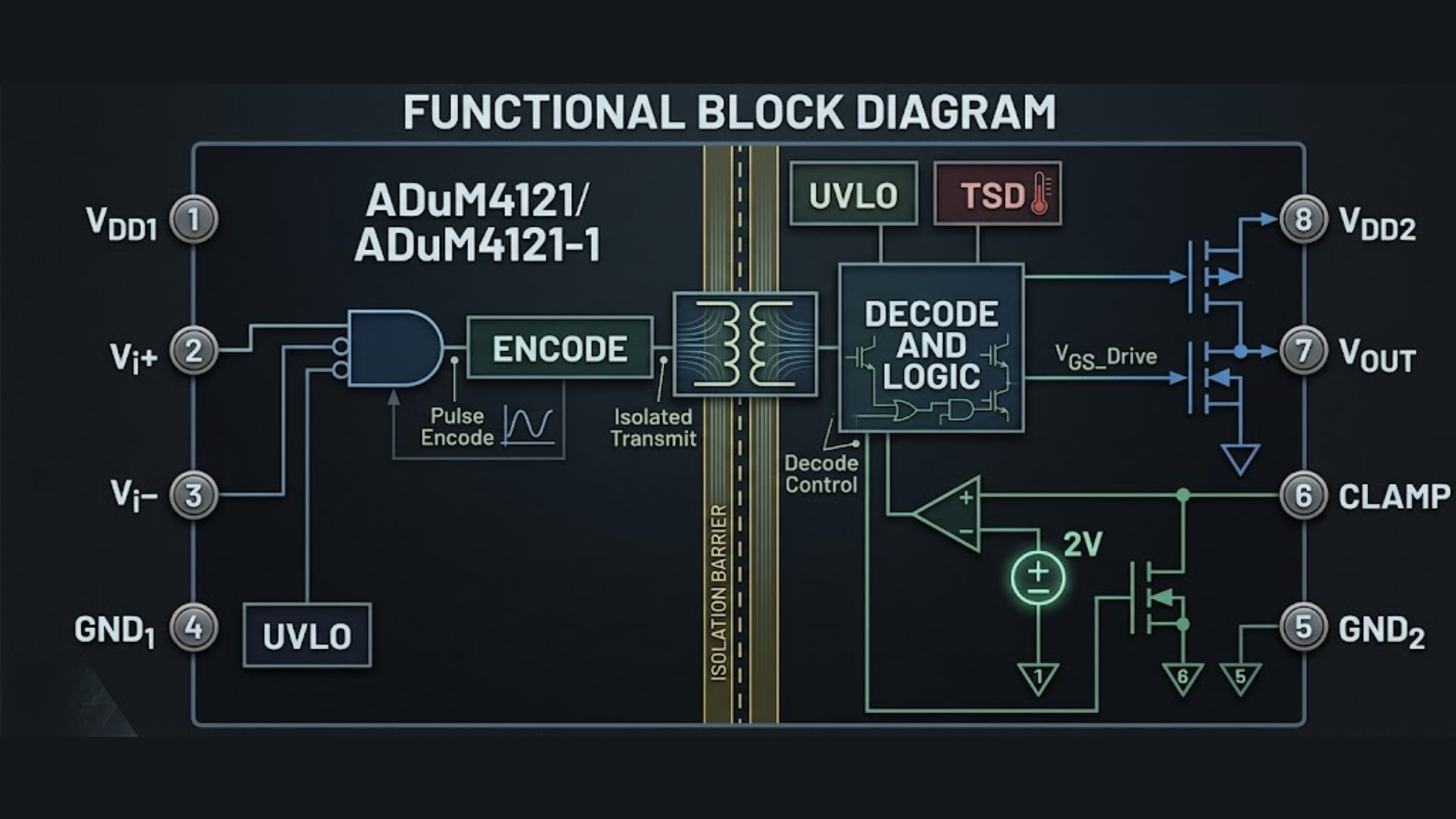
Analog Devices, Inc. (ADI)’s ADuM4121 is a single-channel isolated gate driver with a 2A output capability. The ADuM4121 utilizes ADI’s proprietary iCoupler® technology, providing an isolation barrier using a monolithic transformer isolation architecture. This isolation barrier provides galvanic isolation between a low-voltage control circuit and a high-voltage power switching circuit. In a power converter design, providing an isolation barrier is critical for preventing fault voltage from travelling back into the microcontroller or DSP, as well as for eliminating ground loops between control and power circuits.
This guide provides a complete technical overview of the ADuM4121. It contains the full 8-pin pinout with Operating Conditions, all Electrical Specifications as are found in ADI Data Sheet Rev. 0, as well as a description of the internal Miller clamp and UVLO function, and a Device Variant Selection Guide (ADuM4121 vs. ADuM4121-1). Additionally, the guide includes layout recommendations for printed circuit boards in conjunction with the typical circuit examples for Solar Photovoltaic inverters, Electric Vehicle chargers, Wind Turbine converters, and Battery Energy Storage Systems.
What is the ADuM4121? Device Overview and Product Family
Product Family and Part Numbering
The ADuM4121 and ADuM4121-1 are both single-channel isolated gate drivers with 2 A peak output current. With the same iCoupler® isolation core, both devices have the same 5 kVrms dielectric isolation rating and exhibit greater than 150 kV/μs CMTI performance. The only difference between the two products is thermal protection, with the ADuM4121 incorporating an internal thermal shutdown (TSD) circuit that will drive VOUT low when the junction temperature exceeds approximately 155°C; the ADuM4121-1 does not include TSD circuitry and will not interrupt the gate drive output due to junction temperature.
Both versions of the products can be obtained in tape and reel (ARIZ suffix version), standard versions, and extended industrial temperature range enhanced product (EP) versions are also available. There are three secondary undervoltage lockout (UVLO) threshold options available for each version; these are referred to as Option A at 3.5V, Option B at 6.5V, and Option C at 10.5V. This allows designers to select a suitable UVLO level to match the gate drive supply voltage without requiring additional voltage supervision circuitry.
| Feature | ADuM4121 | ADuM4121-1 |
|---|---|---|
| Output Current (Peak) | 2 A | 2 A |
| Thermal Shutdown (TSD) | ✅ Yes — activates >155°C typ. | ❌ No — output continues above 155°C |
| Internal Miller Clamp | ✅ Yes | ✅ Yes |
| Isolation Rating | 5 kVrms | 5 kVrms |
| Package | 8-lead SOIC (wide body) | 8-lead SOIC (wide body) |
| Input Supply VDD | 12.5 V – 6.5 V | 2.5 V – 6.5 V |
| Output Supply VDD | 24.5 V – 35 V | 4.5 V – 35 V |
| CMTI | >150 kV/μs | >150 kV/μs |
| Propagation Delay (typ.) | ~40 ns | ~40 ns |
| Best Suited For | Safety-critical, high-ambient environments | Lowest latency; external thermal protection available |
iCoupler® Technology: How the Isolation Barrier Works
The ADI iCoupler® replaces the traditional optocoupler’s LED-photodiode pair with on-chip air-core transformers implemented using a standard CMOS process. The primary and secondary windings of the transformer are isolated by a thick polyimide layer, which forms the insulating barrier. Data transmission occurs through magnetic coupling, where a CMOS encoder converts incoming signal edges into high-frequency pulses. These pulses are transferred across the transformer and decoded on the secondary side by a CMOS decoder, which regenerates the original digital signal.
This architecture offers three key advantages over alternative solutions. Compared to optocouplers, iCouplers eliminate LED aging issues, do not require forward current biasing, and provide significantly lower propagation delay (typically 30–50 ns versus 50–200 ns for comparable optocouplers).
Compared to pulse transformer-based designs with discrete driver circuits, the iCoupler is a single-package solution with a single supply, offers deterministic propagation delay, eliminates concerns of transformer core saturation, and does not require external reset circuitry.
In comparison with capacitive-based digital isolators, transformer-based coupling is less susceptible to common-mode transients (CMTI). This is because the parasitic capacitance across the isolation barrier is very low, and the differential transformer coupling effectively rejects common-mode noise that capacitive isolators may inadvertently couple to the output.
ADuM4121 Pinout and Pin Descriptions
Pin Diagram — 8-Lead Wide-Body SOIC
Package Type: SOIC-8W, 8-Lead Wide Body. Creepage distance between Pin 4 (VI−) and Pin 5 (VDD2) is 8mm and meets requirements for Reinforced Isolation.
According to the ADIs datasheets, for safety certification, the device is treated as a Two Terminal Device; therefore, Pins 1 through 4 are shorted together internally on the Primary Side, and Pins 5 through 8 are shorted together internally on the Secondary Side.
The PCB design must ensure full creepage distance between any copper on the primary side and any copper on the secondary side to maintain proper isolation.
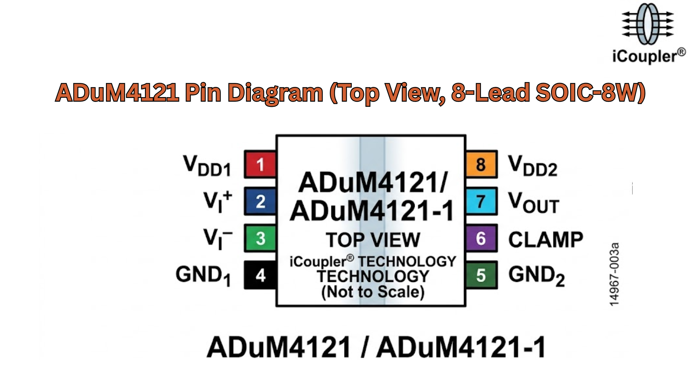
Pin Function Table with Operating Conditions
| Pin No. | Pin Name | Type | Voltage Range | Functional Description |
|---|---|---|---|---|
| 1 | VDD1 | Power Input | 2.5 V – 6.5 V | Primary-side supply voltage. Powers input CMOS logic, iCoupler transmitter coil driver, and UVLO monitor. Decouple with 100 nF ceramic at pin. |
| 2 | GND1 | Ground | 0 V | Primary-side ground. Galvanically isolated from GND2. Do not connect to GND2 on PCB. |
| 3 | VI+ | Logic Input | CMOS (VDD1) | Positive logic input. Accepts active-high PWM when VI− is tied to GND1. Thresholds referenced to VDD1. |
| 4 | VI− | Logic Input | CMOS (VDD1) | Negative logic input. Accepts active-low PWM when VI+ is tied to VDD1. No level shifting required. |
| 5 | VDD2 | Power Input | 4.5 V – 35 V | Secondary-side supply voltage. Powers output stage and receiver. Supports single (+15 V) and dual (+15/−5 V) gate drive. Decouple with 100 nF + 1–10 µF. |
| 6 | GND2 | Ground | 0 V | Secondary-side ground. VOUT referenced here. Isolated from GND1. |
| 7 | VOUT | Driver Output | VDD2 – GND2 | Gate driver output. ±2 A peak. Drives IGBT, Si, SiC, GaN. Forced low under UVLO. |
| 8 | MCLP | Clamp Output | ~2 V (active) | Miller clamp. Activates near 2 V to prevent false turn-on via Cgd. Behavior may vary for ADuM4121-1. |
Dual-Input Logic (VI+ and VI−) Operation
The dual-input format of an ADuM4121 allows for two independent logic polarities to be selected by the designer without any external components being required to configure the system. The way the system operates is based on the input pin used as the active switching condition and the static level on the pin.
| Mode | VI+ State | VI− State | VOUT Behavior | Typical Use Case |
|---|---|---|---|---|
| Positive Logic | Active switching input (PWM) | Tied LOW to GND1 | High = Gate ON; Low = Gate OFF | Standard MCU GPIO / DSP PWM (3.3 V or 5 V) |
| Negative Logic | Tied HIGH to VDD1 | Active switching input (PWM) | Low = Gate ON; High = Gate OFF | Inverted-polarity control signals |
| Enable / Disable | Static HIGH | Static LOW | Output follows VI+ (active high) | Simple enable/disable without PWM controller |
The datasheet specifies propagation delay conditions as the time from the transition of the active input pin to the transition of VOUT at specified load conditions. Channel-to-channel matching, or the maximum variation between multiple ADuM4121s switching, is specified in the datasheet for multi-switch applications where switching symmetry is important.
Key Electrical Specifications and Performance Parameters
Absolute Maximum Ratings and Recommended Operating Conditions
The table below summarizes the major electrical specifications from the ADuM4121/ADuM4121-1 datasheet. Unless specified otherwise, all parameters are considered at a nominal temperature of 25 °C (TA = 25 °C). Derating curves, maximum bipolar and unipolar operating voltage limits, and thermal resistance data can be found in their entirety in the ADuM4121/ADuM4121-1 datasheet.
| Parameter | Min | Typical | Max | Unit | Notes |
|---|---|---|---|---|---|
| VDD1 — Input Supply Voltage | 2.5 | — | 6.5 | V | Primary side; CMOS logic compatible |
| VDD2 — Output Supply Voltage | 4.5 | — | 35 | V | Secondary side; supports wide gate drive range |
| Peak Output Current (VOUT) | — | — | 2.0 | A | Source and sink capability |
| Isolation Voltage (Dielectric) | — | — | 5,000 | Vrms | 1-minute test; reinforced isolation |
| CMTI — Transient Immunity | 150 | — | — | kV/μs | Guaranteed minimum |
| Propagation Delay (tPHL / tPLH) | — | ~40 | — | ns | Typical; see datasheet for max |
| Miller Clamp Threshold | — | 2.0 | — | V | Active on falling edge |
| Primary UVLO Rising | 2.0 | — | — | V | Includes hysteresis |
| Secondary UVLO Rising | — | 3.5 / 6.5 / 10.5 | — | V | Variant dependent |
| Operating Temperature | −40 | — | +125 | °C | Industrial range |
| Thermal Shutdown (ADuM4121) | — | 155 | — | °C | Output forced low |
| Creepage (SOIC Wide) | — | 8 | — | mm | Reinforced isolation geometry |
UVLO (Under-Voltage Lockout) Operation
Under-Voltage Lockout (UVLO) is a protection mechanism that forces the VOUT output to a defined low (off) state whenever the supply voltage on either the primary or secondary side drops below a pre-set threshold. In the ADuM4121, UVLO operates independently on both supply domains:
• Primary-side UVLO: If VDD1 drops below the rising-edge threshold (minimum ~2.0 V), VOUT will be driven low independent of the condition of VI+ or VI−. This avoids undefined gate states during the power-on of the control side or a brown-out situation.
• Secondary-side UVLO: If VDD2 drops below the selected threshold level, VOUT will again be driven low. This is important for situations where the isolated power rail supplying the gate driver circuit will droop during power-up to avoid a partial charge on the gate, driving a shoot-through condition in a half-bridge configuration.
• Hysteresis: Built-in hysteresis prevents output oscillation during slow power-ramp scenarios (e.g., soft-start circuits or capacitor-charged isolated supplies). The output remains locked until VDD clears the hysteresis band above the turn-on threshold.
| Variant Option | VDD2 UVLO Rising Threshold (typ.) | Typical Gate Drive Supply | Application Context |
|---|---|---|---|
| Option A (e.g., ADuM4121ARIZ) | 3.5 V | 5 V single supply | Low-voltage gate drive; 3.3 V / 5 V MOSFET systems |
| Option B (e.g., ADuM4121BRIZ) | 6.5 V | 12 V – 15 V supply | Standard IGBT / Si MOSFET gate drive |
| Option C (e.g., ADuM4121CRIZ) | 10.5 V | 15 V+ supply | SiC MOSFET requiring strict UVLO validation |
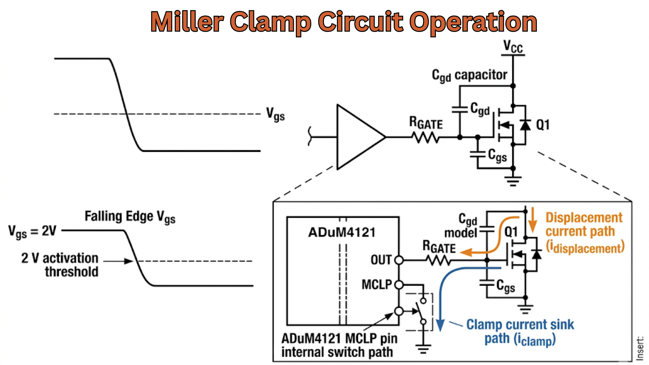
Miller Clamp: Circuit Operation and Why It Matters
The false turn-on problem:
When using a half-bridge configuration for a power stage, the high-side switch of the driver will turn on just as the low-side switch of the driver turns off. This fast dv/dt at the switching node of the power stage will couple to the gate of the low-side device through the Miller capacitance (Cgd for MOSFETs and Cce for IGBTs) of the low-side device. If the current from the coupling of the Miller capacitance creates a voltage at the gate of the low-side device (via RGATE) that is greater than the device threshold voltage, the low-side device will fire spuriously (i.e., the low-side device will turn on) due to Miller-induced false turn-on. If this occurs, both devices may conduct simultaneously, resulting in shoot-through (i.e., both devices conduct at the same time) and catastrophic failure of the devices.
How the ADuM4121 Isolated Gate Driver Miller clamp works:
The internal comparator continuously monitors the VOUT pin. As VOUT begins to turn off (VOUT starts falling), at approximately 2V, an internal low-impedance switch closes and connects the gate terminal directly to GND2 through the Miller clamp path, which presents a lower impedance than RGATE alone. Thus, after being activated at 2V, the clamp can actively sink any charge that would have been injected by Cgd prior to exceeding the gate threshold voltage (i.e., gate threshold voltages for most SiC MOSFETs/MIGBTs are between 2.5–4V).
Why it matters for SiC:
The switching times of SiC MOSFETs are extremely fast, and dv/dt at the switching node is between 10 V/ns and 50 V/ns. This fast transition causes significant displacement currents due to even low levels of Cgd capacitance. While SiC MOSFETs have less gate charge compared to their silicon counterparts, their dv/dt is faster than that of IGBTs, rendering them susceptible to false turn-on. The integrated Miller clamp in the ADuM4121 avoids the need for an additional external clamp transistor.
ADuM4121 vs ADuM4121-1: Which Variant Should You Choose?
Decision Criteria Based on Application Requirements
The choice between ADuM4121 and ADuM4121-1 is primarily governed by whether autonomous thermal protection is required at the gate driver level or whether the system architecture provides equivalent protection externally. The following table maps application requirements to the recommended variant.
| Application Requirement | ADuM4121 (with TSD) | ADuM4121-1 (no TSD) |
|---|---|---|
| Safety-critical system (IEC 61508, ISO 26262) | ✅ Recommended — TSD provides autonomous protection | ❌ Not recommended without external protection |
| High-ambient environment (>85°C chassis) | ✅ TSD activates before damage | ⚠️ Risk without TJ monitoring |
| Minimum propagation delay required | ⚠️ Slightly higher latency | ✅ Lower latency path |
| External MCU/FPGA thermal control | ✅ TSD redundant but safe | ✅ Acceptable alternative |
| EV traction inverter / EV charger | ✅ Best for certification | ❌ External monitoring required |
| Industrial motor drive | ✅ / ❌ Both acceptable | ✅ Acceptable with MCU |
| Lowest unit cost (BOM) | ⚠️ Slightly higher cost | ✅ Lower cost option |
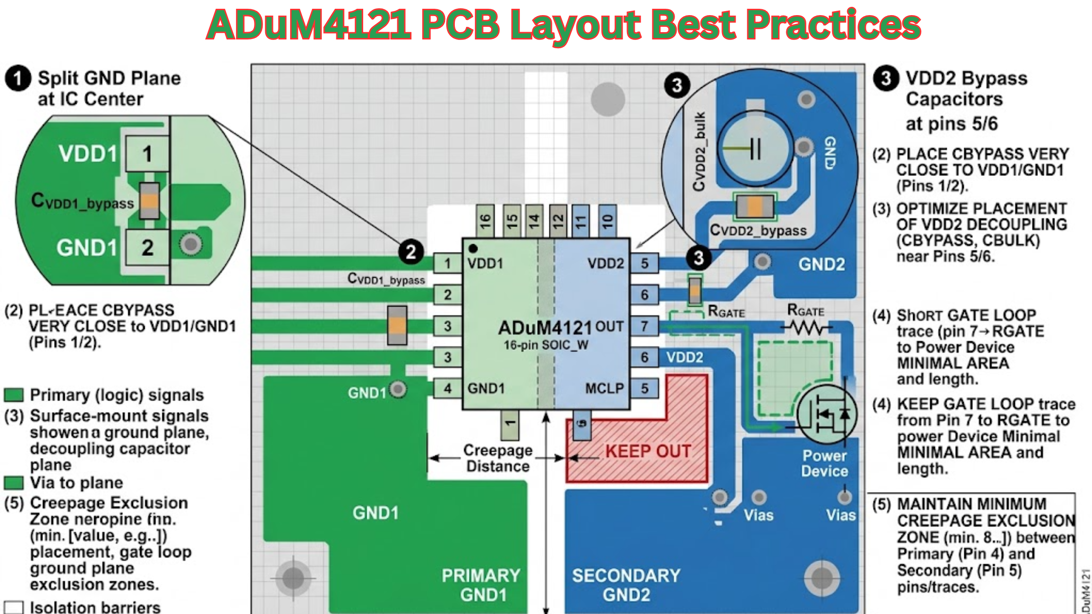
PCB Layout Guidelines and Design Considerations
Decoupling and Supply Bypass
Proper decoupling is the most critical factor at the PCB level that affects the performance of the gate drive signal. During fast transitions (edges) from the ADuM4121 output stage (up to 2A being pulled at the output), this current must be supplied locally through bypass capacitors and cannot be drawn through long PCB traces from a remote bulk supply. Inductance on the supply path causes VDD2 to ‘droop’ during output switching transients, adversely affecting edge rates and potentially causing UVLO operation in borderline supply designs.
• VDD1/GND1: A 100 nF X7R ceramic capacitor should be placed as closely as possible to the VDD1 and GND1 pins. The bypass should be routed directly to the pads by minimizing trace length and the loop area between the capacitor pads and the IC pins in order to reduce effective bypass inductance.
• VDD2/GND2: Place one 100 nF X7R ceramic capacitor for high-frequency decoupling, plus one 1–10 µF ceramic or tantalum bulk capacitor within 2–3 mm of VDD2/GND2. The bulk capacitor supplies the instantaneous 2 A peak demand during gate turn-on events without pulling down the supply rail.
• Via inductance: Avoid routing the bypass loop through vias where possible. A via in a 1.6 mm FR4 board adds approximately 0.5–1.0 nH per via — two vias in the bypass loop can add 1–2 nH, enough to degrade rise time measurably at 2 A switching currents.
Isolation Barrier and Creepage Requirements
The 8 mm creepage distance between Pin 4 (VI−, primary side) and Pin 5 (VDD2, secondary side) is integral to the wide-body SOIC package geometry. The PCB layout is responsible for maintaining — and ideally extending — this clearance in the copper layer design.
- Split ground plane: Do not place a continuous copper ground plane beneath the ADuM4121 device. Instead, divide it into two areas: GND1 and GND2. Place the split in such a manner that the split lies right underneath the body of the ADuM4121 IC in an area that is perpendicular to the pin rows. The gap in the split needs to be 0.5 mm or larger and devoid of copper on both layers.
- No copper in the creepage zone: Do not place copper fills, signal traces, vias, or test points in the region between the primary-side (Pins 1–4) and secondary-side (Pins 5–8) pads. This applies to all copper layers, not just the top layer.
- PCB creepage verification: When reinforced isolation compliance is desired for IEC 60664-1, ensure that the actual copper-to-copper creepage clearance on your PCB design, including solder mask opening width allowance, via placement tolerance, and PCB panel cut-through clearance, equals the minimum creepage required for the working voltage as per Pollution Degree 2.
- Slot option: In high-voltage applications with strict creepage requirements, a PCB slot (typically 2–3 mm wide) may be routed under the IC body to further increase the effective creepage distance. Refer to IEC 60664-1 for detailed creepage calculations for both surface-mount and through-hole designs.
Gate Loop Minimization
Fast current pulses travel around the gate drive loop (from VOUT via RGATE to gate power device, and back to GND2 via source/emitter). These fast current pulses develop inductive voltage overshoots through L × dI/dt. Excess inductance in the gate drive loop degrades the switching waveforms, adds to the switching losses, and causes gate voltage overshoot that can damage or destroy the gate oxide.
| Layout Principle | Implementation | If Violated |
|---|---|---|
| Minimize gate loop | Place driver close to gate | Overshoot, slow edges |
| Wide gate traces | ≥0.5 mm VOUT → RG → Gate | Higher inductance |
| Kelvin source | Separate sense return path | Ground bounce, poor dv/dt |
| RGATE design | Model parasitics (L, Cgs, Ciss) | Ringing or loss increase |
| Separate RGON/RGOFF | Independent turn-on/off control | No EMI/speed tuning |
Green Energy Applications of the ADuM4121
These characteristics of the ADuM4121 make it perfectly suited to tackle the main challenges faced in the power conversion process for green energy sources, namely, galvanic isolation for high voltage buses, resistance to fast switching transient spikes, and prevention of false turn-on conditions in wide bandgap semiconductors.
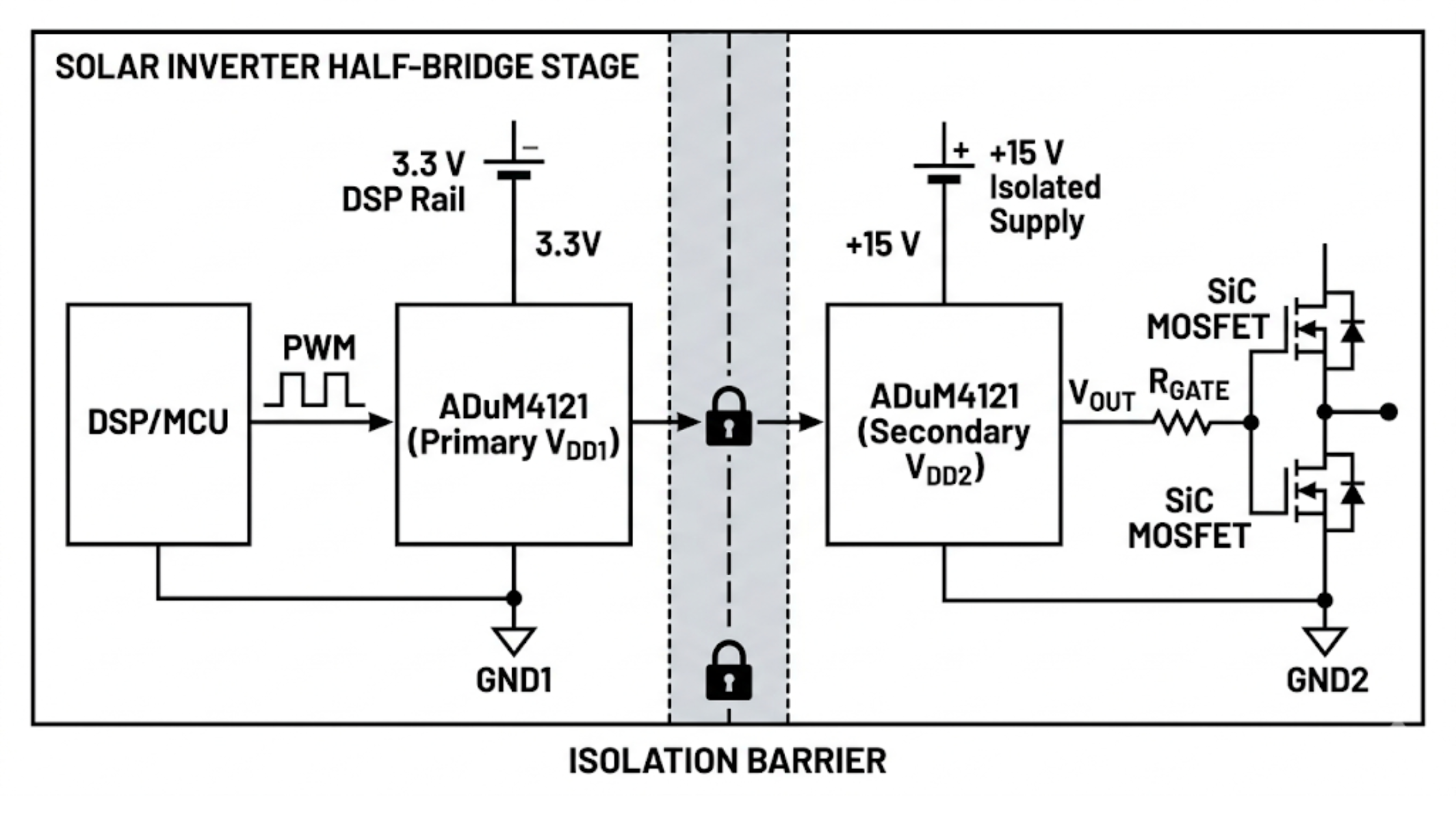
Solar PV String Inverters
Solar String inverters convert the DC output of photovoltaic modules, typically between 600 V and 1500 V (600-1,500 V bus), and convert it into grid-compliant AC voltage. In other words, string inverters are used to convert energy generated by the sun into usable energy for a power grid. The inverter H-bridge (or half-bridge) power stage uses IGBT or, increasingly, SiC MOSFET switches. The ADuM4121 has 5kVrms isolation from the inverter to the DSP or microcontroller, and it can transmit signals across the barrier of the 1,500V DC bus to the 3.3V/5V control domain.
Instead of using the more established IGBT switching device in string inverters, SiC MOSFET switching devices are being used. Switching frequency for SiC MOSFETs is between 20kHz – 100kHz (IGBTs are 4kHz – 16kHz). Therefore, output filter and magnetics sizes associated with string inverter applications are smaller when using SiC MOSFET switching devices than IGBT switching devices. At 20kHz, a 600V switching event (30ns of time for switching) produces a dv/dt value of 20kV/μs, which is significantly less than the ADuM4121’s high (>150kV/μs) CMTI specification. Output corruption would occur from the same switching event in a legacy 10kV-50kV/μs optocoupler due to the high dv/dt value. The ADI evaluation board (EVAL-ADuM4121WHB1Z) demonstrates the performance of the ADuM4121 device in providing drive power to Wolfspeed SiC MOSFETs in a half-bridge topology, which is a power stage topology used in string inverter designs.
ADuM4121 Isolated Gate Driver Parameter Alignment with Solar Inverter Requirements
| Solar Inverter System Requirement | ADuM4121 Specification | Engineering Relevance |
|---|---|---|
| Isolation (600–1500 V DC bus) | 5 kVrms reinforced | Meets IEC 62109; protects DSP/MCU |
| SiC transient immunity | CMTI >150 kV/μs | No false turn-on at high dv/dt |
| High-frequency switching | ~40 ns delay | Accurate PWM at 20–50 kHz |
| Shoot-through prevention | Internal Miller clamp (~2 V) | Removes external clamp circuitry |
| Outdoor operation | −40°C to +125°C | Full solar enclosure temperature range |
| Compact gate drive PCB | 8-lead SOIC package | High power density design |
| Gate drive supply | VDD2: 4.5–35 V | Supports SiC + IGBT gate levels |
EV Charging Infrastructure (On-Board and Off-Board Chargers)
Level 2 AC chargers and DCFCs have two isolated stages: the PFC stage and the isolated DC-DC converter stage that operate at 400 V or 800 V battery bus voltages. Some of the critical criteria for gate driver selection in electric vehicle charging applications are low leakage current over the isolation barrier (important for ground fault detection in electric vehicle charging standards), reliability during rapid load transients due to battery state-of-charge change, and operation in a broad ambient temperature range in outdoor electric vehicle charging stations.
The isolation technology based on transformers used in the ADuM4121 offers significantly reduced leakage current compared to level shift gate drivers that can be considered a crucial parameter in electric vehicle charging applications where leakage current monitoring (IEC 62955, IEC 62752) is mandatory. The dual-supply gate drive scheme (+15 V/−5 V) is common practice in SiC-based DC-DC converter of electric vehicle chargers working at 400-800 V. The VDD2 voltage is supplied by +15 V power line, while GND2 is connected to −5 V supply, and VOUT swings between VDD2 and GND2, thus providing the full-range +15 V/−5 V gate swing without any additional external modifications of the ADuM4121.
Industrial Motor Drives and Wind Turbine Converters
Wind turbine back-to-back converter systems consist of two independently controlled stages: the generator-side converter (GSC), which rectifies variable-frequency AC from the generator into a DC link, and the grid-side converter (GSC), which inverts this DC voltage into fixed-frequency AC for grid injection.
Each converter stage contains multiple power switches, and each switch requires an isolated gate drive channel. The single-channel architecture of the ADuM4121 allows designers to assign one driver per switch position, reducing channel-to-channel interference and simplifying isolated supply management.
UVLO for shoot-through protection: In many motor drive and power conversion systems, isolated gate driver supplies are generated using bootstrap circuits or compact isolated DC-DC converters. During startup, these supplies may rise slowly. The secondary-side UVLO of the ADuM4121 ensures that VOUT remains low until VDD2 is fully established, preventing partial gate drive signals during power-up and eliminating the risk of shoot-through in half-bridge configurations.
Battery Energy Storage Systems (BESS)
Grid-scale and commercial BESS use bidirectional DC-DC converters (battery ↔ DC bus) and bidirectional inverters (DC bus ↔ AC grid). These systems must handle large common-mode disturbances introduced by long cable runs between the battery stack and the power converter — cable lengths of 5–20 meters are not uncommon in large installations, and the capacitive coupling of switching transients along cable shields can generate common-mode impulses well exceeding 10 kV/μs at the gate driver input.
The ADuM4121, with a CMTI rating greater than 150 kV/μs, provides a safety margin of approximately 10–15× over these disturbance levels. This eliminates the need for additional filtering of gate drive signals while maintaining signal integrity under harsh electrical conditions. In addition, the device’s dual-input logic (VI+ / VI−) simplifies interfacing with bidirectional PWM controllers by directly supporting complementary control signals without requiring external inversion.
Safety Certifications and Regulatory Compliance
Isolation Standards and Certifications
The ADuM4121/ADuM4121-1 is intended to meet the following certification levels, as defined in the applicable industry standards. At the time of publication of the Rev. 0 datasheet, some certifications were pending approval. Certified engineers who wish to integrate the ADuM4121 into their products that are safety certified (CE marking, UL listing, IECEx) are encouraged to verify that the ADuM4121 will continue to meet the current certification requirements by contacting ADI or checking the ADI product page; due to the manner in which certification evolves after the original product release, there may have been changes to certification status.
Isolation Voltage and Safety Parameters
| Parameter | Value | Test Condition / Standard |
|---|---|---|
| Rated Dielectric Isolation Voltage | 5,000 Vrms | 1-minute test per IEC 60747-17 |
| Partial Discharge Extinction Voltage | ≥1,200 Vp | VDE 0884-11 |
| Isolation Class | Reinforced Isolation | IEC 60664-1 (not basic isolation) |
| Pollution Degree | 2 | IEC 60664-1 Table A.2 |
| Working Voltage (bipolar AC) | Refer curve | Fig. 28/29 — higher stress case |
| Working Voltage (unipolar DC/AC) | Higher than bipolar | Fig. 29 — reduced insulation stress |
| Projected Service Life | 50-year target | ADI accelerated life testing |
| Certifying Bodies | UL, CSA, VDE, ATEX | Status pending (datasheet Rev. 0) |
Reinforced vs Basic Isolation — Why It Matters:
Reinforced isolation consists of one layer of protection, which is equal in level of protection to double insulation (two layers of basic insulation connected in series) due to the design and testing requirements. Therefore, when the ADuM4121 is used as an isolation barrier at the primary level, no additional isolating device is needed in series for compliance with end product requirements. In contrast to the ADuM4121’s reinforced rating, basic isolation requires another layer to achieve reinforced protection. The ADuM4121’s reinforced certification simplifies the safety architecture and lowers the number of parts needed on the bill of materials (BOM).
Accelerated Life Testing and 50-Year Service Life:
ADI’s life testing methodology applies voltages higher than the rated working voltage and uses acceleration factors to calculate time-to-failure at actual operating conditions. For unipolar (DC or single-polarity AC) waveforms, the dielectric stress on the polyimide isolation layer is significantly lower than for bipolar AC, allowing operation at higher working voltages while maintaining the 50-year service life design target. Any cross-insulation voltage waveform that does not conform to unipolar classification must be treated as bipolar AC for conservative isolation design.
Frequently Asked Questions (PAA Targeting)
ADuM4121 includes an integrated Miller clamp and uses an 8-pin package, while ADuM4120 omits the Miller clamp and uses a smaller 6-pin package. Both share 5 kVrms isolation and >150 kV/μs CMTI.
Yes. It supports enhancement-mode GaN devices with 2 A drive current and fast switching. External negative supply is needed if negative gate turn-off is required.
CMTI is immunity to high dv/dt across the isolation barrier. >150 kV/μs ensures reliable operation in fast-switching SiC systems and prevents false triggering.
Use 100 nF X7R capacitors at both supply pins and a 1 µF bulk capacitor on VDD2 for stable gate drive performance.
Yes. It supports reinforced isolation with a 5 kVrms rating, provided PCB creepage and safety design rules are followed.
Conclusion: Is the ADuM4121 the Right Isolated Gate Driver for Your Design?
If you have made it through this entire guide, you now have a clearer picture of what the ADuM4121 actually does under the hood — not in terms of marketing language, but in terms of real circuit behavior. You understand why the Miller clamp activates at 2 V and not at zero. You understand why the choice between ADuM4121 and ADuM4121-1 is not just a checkbox on a spec sheet but a decision that directly affects how your system behaves during a thermal fault. And you understand why >150 kV/μs CMTI matters when your SiC MOSFET is switching 600 V in 30 nanoseconds.
That kind of depth is not just useful for passing a design review — it is what separates a gate drive circuit that works in the lab from one that survives in the field, at temperature, over years of switching cycles, in a solar inverter on a rooftop in July or in an EV charger on a motorway in December.
What the ADuM4121 Actually Delivers — Technically
Step back from the individual specifications and look at what this IC actually solves as a system-level component:
Where the ADuM4121 Fits Best — and Where It Does Not
No component is the right answer for every problem. Part of engineering judgment is knowing where a device belongs and where a different solution is more appropriate. Here is an unvarnished assessment:
The Green Energy Context: Why Gate Driver Selection Matters at Scale
It is worth stepping back from the circuit level and acknowledging the broader context that makes this component selection genuinely significant. The world is in the middle of a large-scale energy transition. Solar capacity is being deployed at gigawatt scale. EV charging infrastructure is being built out across continents. Battery storage systems are being installed next to wind farms, substations, and commercial buildings. Every single kilowatt of that capacity passes through a power converter. Every power converter has at least one gate driver.
The efficiency of a power converter is directly affected by gate drive quality. When a gate driver has poor propagation delay consistency, it introduces switching timing errors. Consequently, dead time must be widened to compensate, meaning both switches in a half-bridge overlap in the off state longer than necessary, increasing conduction losses.
In cases where a gate driver provides insufficient CMTI, false turn-on events can occur. These create brief shoot-through current pulses, and since they are repeated at the switching frequency, each pulse deposits energy as heat into the switch junction.
The absence of Miller clamp protection in a fast-switching SiC stage can lead to intermittent false firing. While this does not cause immediate failure, it manifests as accelerated gate oxide wear over thousands of operating hours.
None of these failure modes appear on a nameplate efficiency rating. They accumulate silently, in the field, at scale. Choosing a gate driver like the ADuM4121 — with documented CMTI margins, integrated Miller clamp, precise propagation delay, and a credible isolation rating — is not overspecification. For green energy applications, it is the appropriate level of engineering rigor.
Final Recommendations by Application
Based on the technical analysis across this guide, here are application-specific recommendations for engineers evaluating the ADuM4121:
| Application | Variant | Key Note |
|---|---|---|
| PV Inverter (SiC >20 kHz) | ADuM4121 TSD B/C | ±15 V / −5 V, check CMTI vs dv/dt |
| EV OBC (400–800 V) | ADuM4121 TSD C | IEC 62752, ISO 26262 TSD required |
| DC Fast Charger | ADuM4121 TSD B/C | Creepage + split supply required |
| Wind Converter (690 V) | ADuM4121 TSD B | −5 V bias, UVLO safe startup |
| BESS (1000 V) | ADuM4121 TSD C | Tune RGON/RGOFF, high CMTI needed |
| Motor Drive (480 V) | ADuM4121-1 B | MCU thermal monitoring required |
COMMENTS