Introduction
Power semiconductor devices such as MOSFETs, IGBTs, GaN transistors, and SiC MOSFETs are heart of modern power electronic systems. Engineers use these devices in power conversion applications ranging from electric vehicles and motor drives to data centers and renewable energy systems. However, these power switches require a gate driver to provide the necessary voltage and current for proper switching operation.
A gate driver serves as an interface between microcontroller and power semiconductor. It supplies required current and voltage to charge and discharge a gate capacitor. In power conversion applications, gate driver design directly affects efficiency, switching losses, electromagnetic interference (EMI), and overall system reliability.
In contrast, a poor gate driver design leads to excessive heating, shoot-through, and catastrophic failure. Hence, gate driver design plays an essential role in reliable and efficient power electronics systems. This article explains operation of gate drivers, different types of drivers used in power conversion applications and their selection criteria, design consideration, and real-world applications.
What is a Gate Driver?
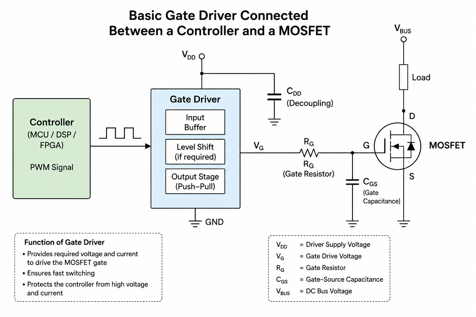
As shown in Fig-1, It is an electronic circuit used to control the switching of power semiconductor devices. It receives signals from the controller and provides sufficient current and voltage to turn the switch ON and OFF.
Gates of power semiconductors possess significant gate capacitance, and it requires current to charge and discharge the gate. A higher gate current allows faster charging, hence leading to faster switching. The following equation determines gate current.
\[I_G=C_G\frac{dV_G}{dt}\]
Here, IG represents gate current, CG represents gate capacitance, and VG is gate voltage. Gate drivers typically perform several functions such as dead-time generation, voltage level shifting, isolation, etc.
Importance of Gate Drivers
The efficiency of a power conversion systems highly depends on its switching characteristics. The gate driver defines how fast a device transitions between the states (OFF and ON) and it directly reflects the overall switching losses.
The following equation determines the switching losses.
\[P_{sw}=\frac{1}{2}VI(t_r+t_f)f_s\]
Where V and I represent voltage and current, while tr and tf and fs are risetime, fall time and switching frequency, respectively. From the given equation, longer switching time increases the losses and reduce the converter efficiency. In other words, a weak driver causes slow turn-on and turn-off, larger EMI emissions, increased heat and losses.
For example, A SiC MOSFET driven by a 1A gate driver and operating at 60 kHz may dissipate substantial switching energy, if driver current is insufficient. In contrast, increasing the driver capability (from 1A to 4A) can significantly reduce the switching losses.
Type of Gate Drivers
Generally, gate drivers are divided based on their circuit configuration and applications. The following subsections present the most common type of gate drivers used in power conversion applications.
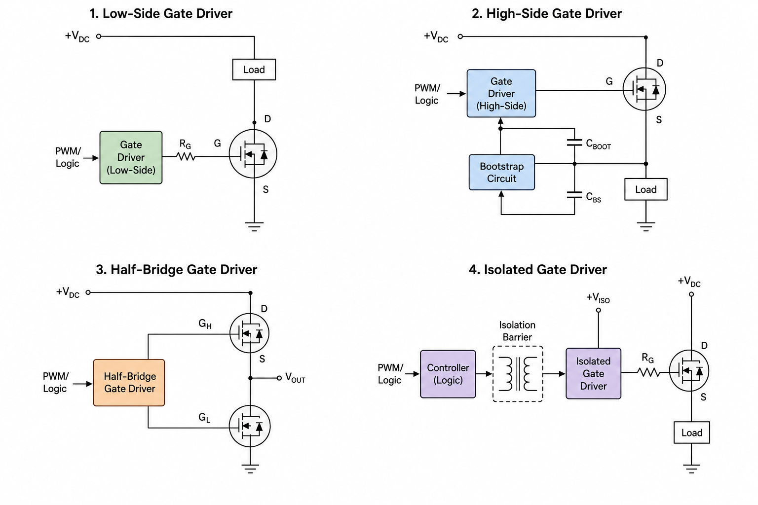
Low-Side Gate Driver
These drivers control the power semiconductor devices connected between the load and ground (See Fig-2). They have a simple design and provide a cost-effective solution. Since, the source terminal is referenced to ground, galvanic isolation is generally not required.
Low-side gate drivers are mainly used in LED drivers, DC-DC converters and low voltage power supplies. A practical example of a low-side gate driver is the Texas Instruments UCC27524D, which is designed to drive MOSFETs and IGBTs in high-speed switching applications.
High-Side Gate Driver
High side gate drivers control the switches connected to the positive DC bus (See Fig-2). As the source voltage changes during switching, additional circuitry such as, bootstrap circuit is required.
The main applications for such drivers are buck converters, motor drives, and half bridge circuits.
Half-Bridge Gate Driver
These gate drivers control both high-side and low-side power semiconductor devices (See Fig-2). They also offer shoot-through protection, dead-time control, and level shifting (For example: 2ED21814S06J by Infineon). Their applications include LLC converters, motor drives, inverters, etc.
Isolated Gate Driver
Isolated gate drivers provide isolation between power and control stage (See Fig-2). This isolation protects controllers, low-voltage electronics, etc. from harmful voltages. These drivers employ several isolation technologies such as transformer isolation, capacitive isolation, and optical isolation.
Owing to their ability to handle higher voltages, these are widely used in industrial drivers, EV inverters, and high-power converters.
Comparison of Gate Drivers
| Driver Type | Advantages | Limitations | Applications |
| Low-Side | Simple and low cost | Ground referenced only | Buck converters |
| High-Side | Controls upper switch | Requires bootstrap circuit | Motor drives |
| Half-Bridge | Drives two switches | More complex | Inverters |
| Isolated | High-voltage protection | Higher cost | EV and industrial systems |
Gate Driver Selection Parameters
Selection of gate drivers for a specific design requires evaluation of several important parameters.
Gate Voltage Requirement
One of the most important parameter is gate voltage. Each power semiconductor device requires a different gate voltage.
| Device | Typical Gate Voltage |
| Silicon MOSFET | 10 to 15 V |
| IGBT | 15 V |
| SiC MOSFET | +15 to +20 V |
| GaN HEMT | -3 to +6 V |
It is essential to supply a correct voltage to avoid device damage and performance degradation.
Peak Gate Current
As discussed, gate drivers must be capable of supplying enough current to charge and discharge the gate rapidly. The following equation calculates the gate current.
\[I_G=\frac{Q_G}{t_{sw}}\]
Here, QG represents total gate charge and Tsw is desired switching time.
Propagation Delay
It is the time between input control signal and the driver output. Propagation delay is selected based on the switching frequency and timing requirements of the application. In half-bridge circuits, matching the propagation delay between high-side and low-side is highly essential to maintain proper dead time and avoid shoot-through.
Also, for high-frequency power converters, a low propagation delay is preferred to ensure accurate switching and minimal mismatch between devices. It is worth noting that excessive delay can lead to increased switching losses, and potential reliability issues.
Common Mode Transient Immunity (CMTI)
This parameter is particularly important in GaN converters, SiC inverters, and motor drives. A higher CMTI rating improves noise immunity and prevents false turn-on caused by rapid voltage transitions. Modern devices such as SiC and GaN generate extremely fast voltage transitions and high CMTI helps the driver to withstand high dv/dt without false switching.
Practical Design Considerations
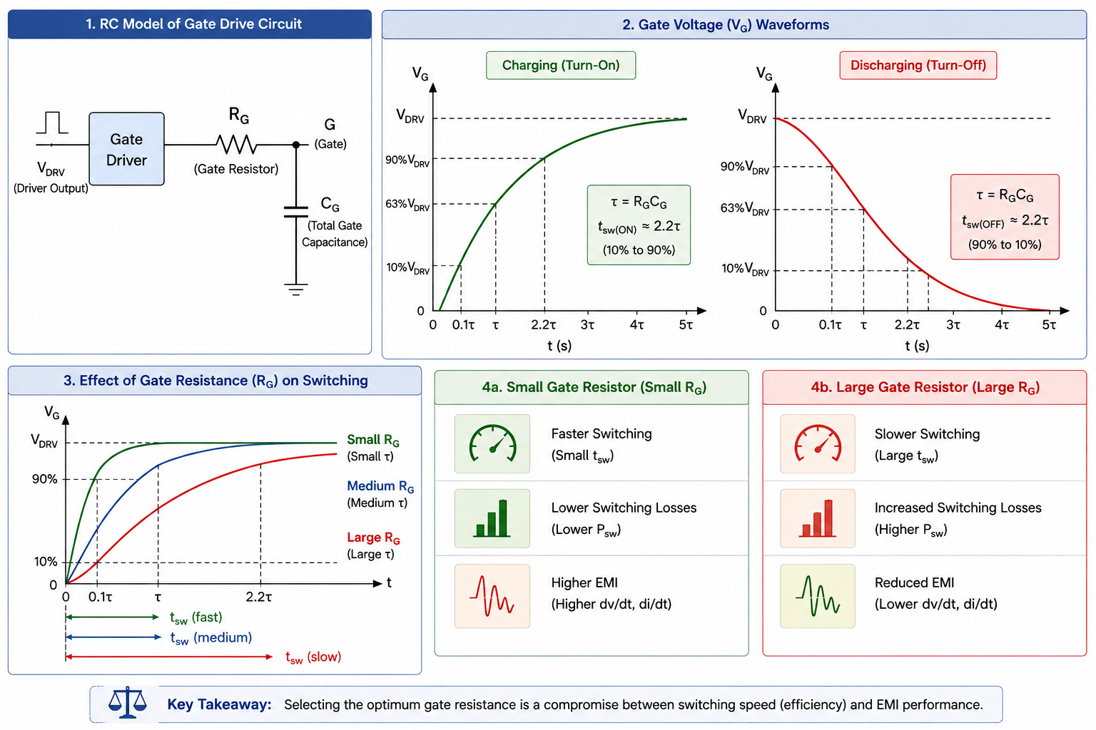
Selection of Gate Resistance
Gate resistors directly influence switching speed of power semiconductor devices. As shown in Fig-3, The gate resistor along with gate capacitor forms a typical RC circuit.This means that the smaller gate resistor will help in faster switching, while a larger gate resistors slows switching thus increasing the switching losses.
Apart from switching speed, the gate resistors also influence EMI. Faster switching leads to higher EMI and vice versa. Therefore, selecting the optimum gate resistance is a compromise.
Dead Time Design
A proper selection of dead time prevents simultaneous conduction of upper and lower switches. Hence, dead time selection is very essential to ensure proper operation. Besides, excessive dead time increases conduction losses and reduce overall efficiency. It is important to note that modern gate drivers often have adjustable dead time to optimize performance.
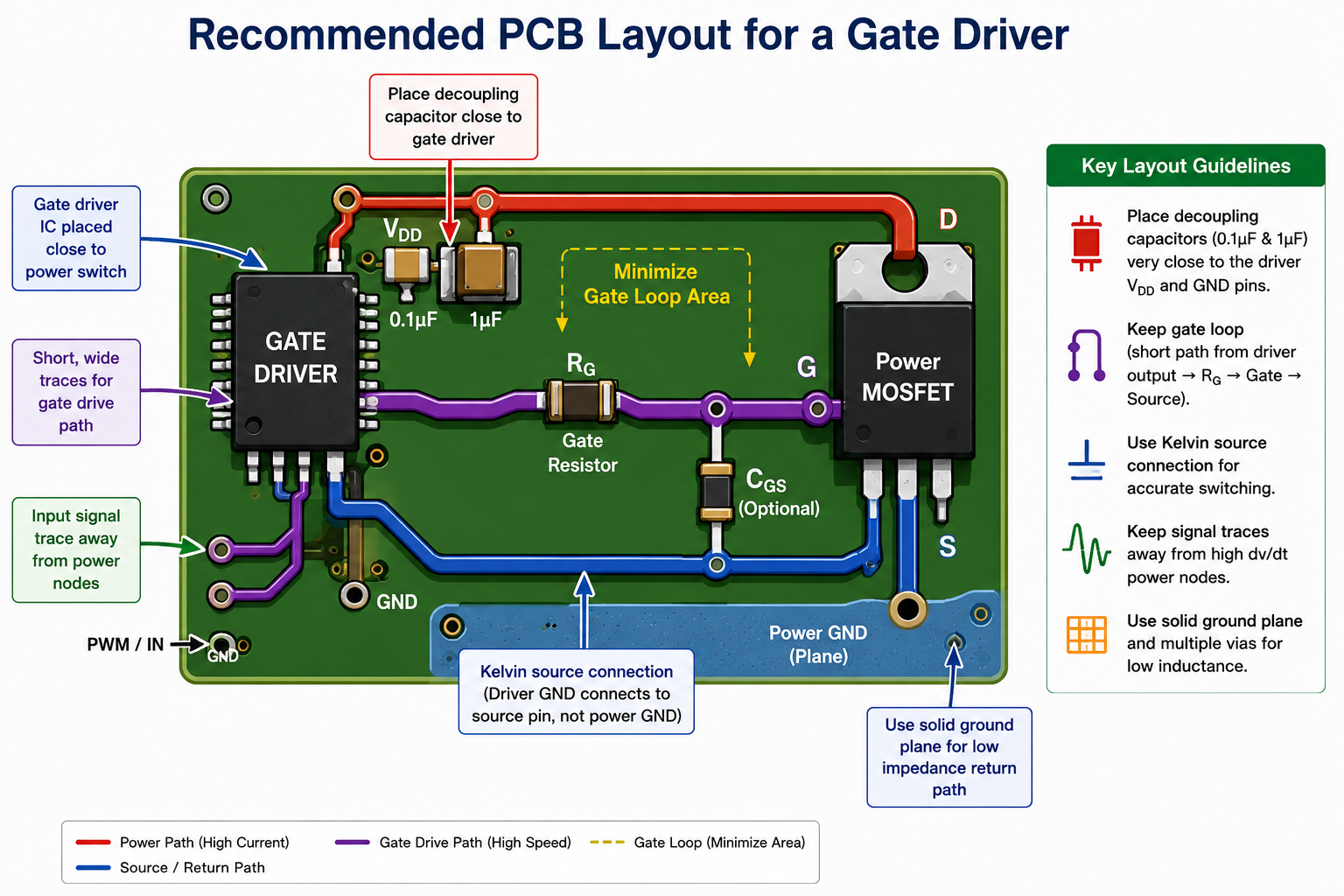
PCB Layout
PCB layout is extremely important when designing a gate driver circuit. A poor PCB layout can degrade the performance of driver circuit. Following are key considerations when designing driver circuit.
- Minimize the gate loop area
- Place the driver close to the switch
- Use short gate traces
- Employ kelvin source connections
- Place decoupling capacitors near the driver
Fig-4 illustrates a typical PCB layout for a gate driver circuit.
Application of Gate Drivers
Gate drivers are widely used in several power electronics systems where reliable and efficient switching is required. Based on the types of gate drivers, following table summarizes common applications and the corresponding gate driver types used in each case.
| Application | Gate Driver Type | Description |
| DC-DC Converters | Low-Side / High-Side | Used in buck, boost, and synchronous converters for efficient power regulation |
| Motor Drives | Half-Bridge / Isolated | Controls inverter switches for AC motor operation |
| Electric Vehicle (EV) Inverters | Isolated | Provides high-voltage isolation and protection in traction systems |
| Solar Inverters | Isolated / Half-Bridge | Converts DC from solar panels to AC for grid or load |
| LED Drivers | Low-Side | Simple and cost-effective switching for lighting applications |
| Battery Chargers | Low-Side / Half-Bridge | Used in fast chargers and power adapters |
| Data Center Power Supplies | High-Side / Half-Bridge | Ensures high efficiency and compact design |
| Industrial Power Systems | Isolated | Provides safety and reliability in high-voltage environments |
Case Study 1: Driver Selection for 5kW SiC inverter
Design Requirements
The project requires a reliable and efficient 5kW SiC inverter. The key requirements are:
- 800V DC bus voltage
- Higher switching frequency to improve power density
- Minimize switching losses and EMI
- Proper isolation for safe operation
Design Approach
As provided in requirements, an isolated gate driver is selected to meet the specified demands.
The driver should provide a gate voltage of +18V and -5V (turn-on and turn-off). During the high-speed switching, dv/dt can induce unwanted gate voltages due to parasitic capacitance. The negative voltage helps in preventing unintended turn-on due to high dv/dt issues and improves noise immunity. This Further ensures the reliable and stable operation.
As discussed, gate current depends on gate charge (QG) and desired switching time. Assuming typical SiC MOSFET with total gate charge of 120nC and desired switching time of 30ns, the gate current will be:
\[I_G=\frac{120 \times 10^{-9}}{30 \times 10^{-9}}=4~\text{A}\]
This means that the gate driver should be able to deliver of at least 4A peak current to achieve fast switching. However, in practical design designers typically select higher values such as 6–10 A to account for parasitic effects (such as UCC27611DRVR).
In addition, higher switching currents lead to faster switching and thus reducing overall switching losses. Gate driver may also integrate advance features such as fault protection, CMTI, etc. these features enhance the reliability of the inverter and simplify overall design.
Case Study 2: 240 W GaN Fast Charger
Design Requirements
A 240 W GaN fast charger needs to be designed. The design requirements are:
- Compact size
- Small magnetic components
- High switching frequency
Design Approach
Considering the load requirements, a low-voltage gate driver with a 5V output can be selected to match the gate requirements of GaN devices. Although GaN transistors exhibit lower gate charge compared to conventional silicon (Si) devices, their extremely fast switching capability requires the gate driver to deliver high peak current (typically 3A-6A range). This enables fast charging and discharging of gate capacitance, minimizing switching losses and supporting high-frequency operation.
The propagation delay is another important factor with GaN devices. The propagation delay should be lower, typically less than 50ns. In addition, proper PCB layout and reduction of parasitic inductance are essential to achieve optimal switching performance.
Common Gate Driver Design Mistakes
| Design Mistake | Consequence |
| Low driver current | Slow switching |
| Large gate resistance | Increased losses |
| Poor PCB layout | EMI problems |
| Improper dead time | Shoot-through |
| Incorrect gate voltage | Device damage |
| Lack of isolation | Controller failure |
Future Trends in Gate Drivers
Gate drivers continue to evolve to satisfy the demands of modern power electronics systems. The following subsections highlight the key developments in advanced gate drivers.
Emerging Technologies
- Integrated drivers
- Digital isolation
- Intelligent protection,
- SiC-specific drivers
- GaN-optimized drivers
Integrated Features
- Desaturation protection
- Temperature monitoring
- Fault reporting
- Adaptive dead-time control
Conclusions
Gate drivers are an essential part of modern power conversion systems. They control the switching behaviour of power semiconductors such as MOSFETs, IGBTs, GaN devices, etc. They determine switching speed, reliability, efficiency, and electromagnetic performance of the system. Therefore, selecting a proper gate driver is critical to achieving optimum system performance.
This article highlights the key parameters for designing the gate drivers, including gate voltage requirements, driver current capability, isolation requirements, propagation delay, and CMTI. Besides, practical considerations such as dead time, PCB layout, and gate resistance were examined to highlight their impact on switching performance and system reliability.
As power converters continue to evolve towards higher switching frequency and power density, gate driver will play an even more important role in converter design. Whether designing a motor drive, solar converter, EV inverter, or a high frequency GaN chargers, understanding gate drivers helps engineers to reduce losses, improve efficiency, and develop more reliable power electronics systems.
Frequently Asked Questions (FAQs)
A gate driver acts as an interface between the controller and the power semiconductor device. It provides the required voltage and current to rapidly charge and discharge the device gate, enabling efficient switching and reducing power losses.
Most microcontrollers cannot supply sufficient voltage or current to drive power semiconductor devices efficiently. A gate driver boosts the control signal and provides the necessary drive capability to achieve fast and reliable switching.
The required driver current depends on the device gate charge and the desired switching time. Devices operating at high switching frequencies generally require gate drivers with higher peak current capability to minimize switching losses.
Non-isolated gate drivers share the same ground reference as the controller and are commonly used in low-voltage applications. Isolated gate drivers provide galvanic isolation between the control circuit and the power stage, improving safety and protecting low-voltage electronics in high-voltage systems.
Gate resistance controls the charging and discharging speed of the gate capacitance. Smaller gate resistors provide faster switching and lower losses but may increase EMI. Larger resistors reduce EMI but can increase switching losses.
Dead time is the delay introduced between turning OFF one switch and turning ON the complementary switch in a half-bridge or inverter circuit. Proper dead time prevents shoot-through current and improves system reliability.
SiC and GaN devices switch very rapidly and generate high dv/dt transients. Isolated gate drivers provide better noise immunity, higher common-mode transient immunity (CMTI), and improved protection for low-voltage control circuits.
Gate drivers are widely used in electric vehicle inverters, motor drives, solar inverters, DC-DC converters, battery chargers, data center power supplies, and industrial power conversion systems.
COMMENTS