1. Introduction
The Altera EP2C35F484C7N, as a part of the Cyclone II family, is known as a mid-range Field-Programmable Gate Array (FPGA). This device is designed for cost-sensitive embedded systems and Digital Signal Processing (DSP) applications.
Historically, the Cyclone II family, introduced by the Altera company (now Intel) in 2004. This family could revolutionize the low-budget FPGAs applications by delivering significantly higher logic density and better performance than previous-generation devices. Additionally, the Cyclone II family could maintain competitive pricing.
Specifically, the Altera EP2C35F484C7N has been able to bridge the gap between low-cost Complex Programmable Logic Devices (CPLDs) and high-performance FPGAs. This device, with its specific features of 33K logic elements, 105 M4K memory blocks, embedded multipliers, and flexible I/O, offers an excellent balance of performance and cost-effectiveness.
This article provides descriptive information about the architecture, internal logic structure, memory blocks, and practical applications of the Altera EP2C35F484C7N FPGA.
2. Cyclone II FPGA Architecture Overview (EP2C35 Series)
The Cyclone II family FPGAs are manufactured on 300-mm wafers using 90-nm low-k dielectric CMOS (Complementary Metal-Oxide-Semiconductor) process technology.
The 90nm node provides an optimal balance:
- Lower manufacturing costs than 130 nm and 350 nm predecessors (e.g., Altera FLEX 10K Series FPGA) due to minimizing silicon area.
- Better power efficiency than older nodes.
- A mature, stable fabrication process with proven reliability.
Therefore, according to Altera’s device-family documentation, Cyclone II FPGAs offer 60% higher performance and half the power consumption of competing 90-nm FPGAs. We can refer to some examples.
2.1 Hierarchical Structure
Essentially, the Cyclone II architecture contains some components and organizes these resources as a hierarchy:
- Logic Elements (LEs)
- Logic Array Blocks (LABs)
- M4K Memory Blocks
- Embedded Multipliers
- Phase-Locked Loops (PLLs)
- I/O Elements (IOEs)
- Interconnect Network
Moreover, Cyclone II devices contain a two-dimensional row- and column-based architecture to implement custom logic. Column and row interconnects of varying speeds provide signal interconnects between Logic Array Block (LAB), embedded memory blocks, and embedded multipliers.
2.2 Logic Resources
The primary computational resource is the Logic Array Block (LAB). Each LAB contains a set of 16 Logic Elements (LEs), carry chains, and local interconnects.
2.2.1 Logic Elements (LEs)
The LE is the smallest unit of logic in the Cyclone II architecture.
Briefly, each LE includes:
- A 4-input Look-Up Table (LUT) that can implement any function of four input variables (function generator)
- A programmable register (Flip-Flop)
- A carry chain connection for high-speed arithmetic operations
- A register chain connection for efficient shift register implementation
- The ability to drive all types of interconnects
Figure 1 shows the block diagram of a Cyclone II family’s logic element.
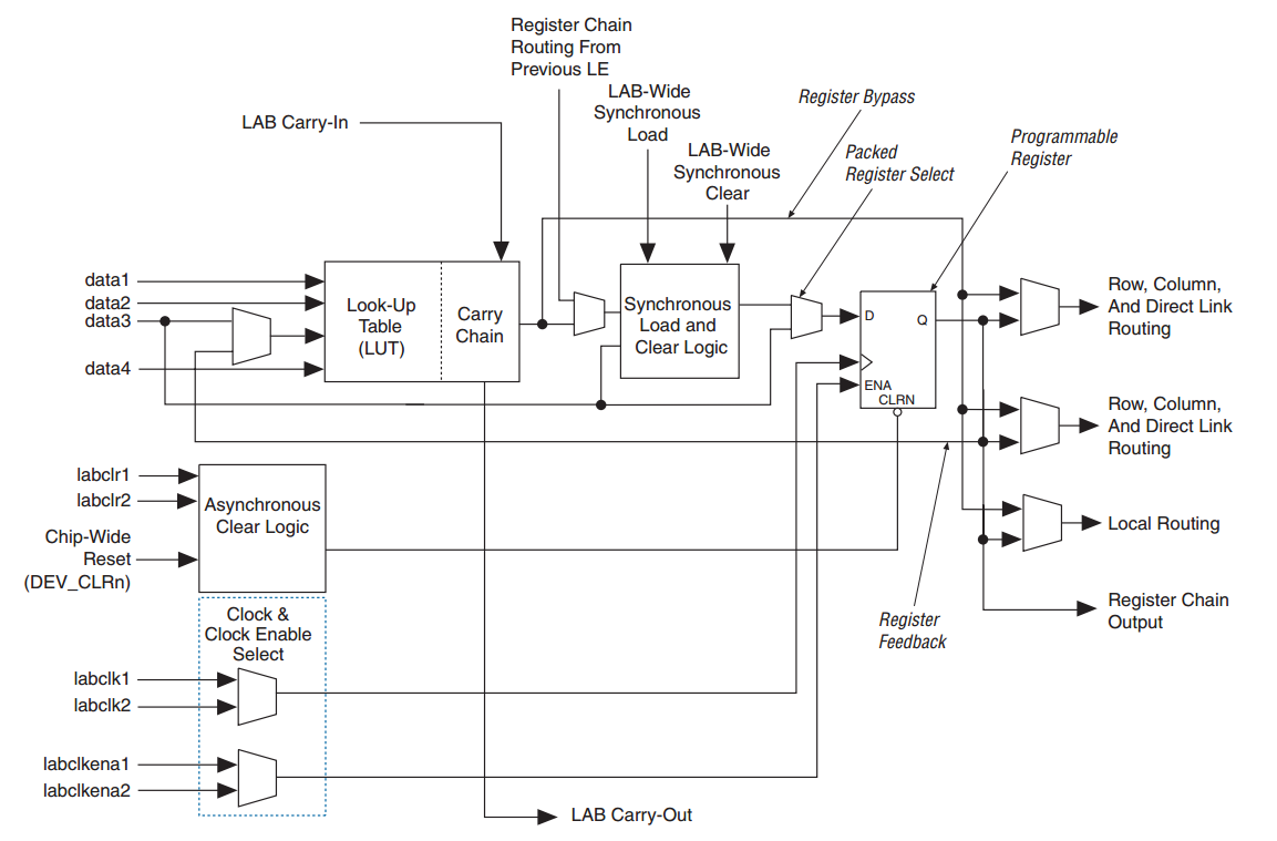
The LE structure allows for both combinational and registered logic. The 4-Input LUT can also be configured as distributed RAM (16×1). When the LUT is configured for purely combinational logic, its output bypasses the register.
Each LE provides three independent outputs:
- Local routing network
- Row and column routing or direct-link interconnects
This feature supports “register packing” allowing the LUT and the register to drive separate routing paths for unrelated tasks. This possibility increases logic density.
The carry chain is a dedicated low-latency path that links all LEs within an LAB and extends across adjacent LABs for high-performance adders, counters, and comparators.
The register chain allows the registers of multiple LEs in the same LAB to be cascaded into compact shift registers or delay lines without consuming general routing resources. This feature is effective for DSP pipelines and data alignment.
The Cyclone II LE is able to operate in two main modes:
- Normal mode: Suitable for general logic applications and combinational functions.
- Arithmetic mode: Ideal for implementing adders, counters, accumulators, and comparators.
2.2.2 Logic Array Block (LAB) Structure
The logic array consists of LABs, with 16 logic elements (LEs) in each LAB. LABs are grouped into rows and columns across the device.
Each LAB also consists of:
- LAB-wide control signals (clocks, enables, clears)
- LE carry chain and register chain connections
- Local interconnect for fast LE-to-LE connections within each LAB
Figure 2 shows the Cylclone II LAB.
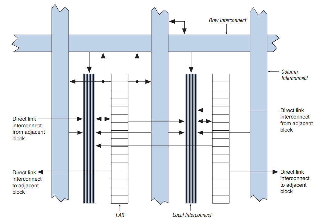
The LAB local interconnect can drive LEs within the same LAB. On the other hand, both row and column interconnects and also LE outputs within each LAB can drive local interconnect of the LAB.
2.3 Memory Blocks (M4K RAM)
The Cyclone II embedded M4K memory blocks are true dual-port dedicated memory blocks with 4 kilobits (4,096 bits) of on-chip Static RAM memory plus 512 parity bits (totally 4,608 bits). These blocks are arranged in columns across the device in between certain LABs.
These blocks can provide dedicated true dual-port, simple dual-port, or single-port memory.
M4K memory blocks offer twice the capacity and expanded performance over their predecessors Embedded Array Blocks (EABs) in the previous generation FLEX 10K series.
Figure 3 shows the M4K block to logic array interface.
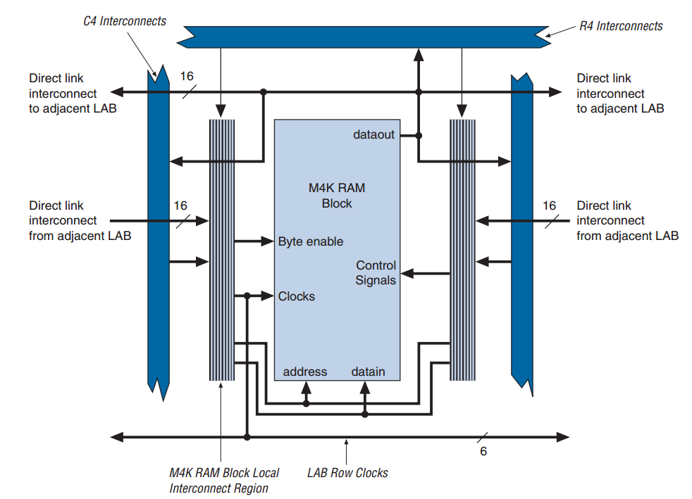
M4K blocks support some functionalities like:
- Up to 250-MHz performance
- Built-in first-in first-out (FIFO) buffers
- Configurable width and depth (aspect ratios)
- Input and output registers (output registers can be bypassed, but input registers cannot)
The M4K blocks can communicate with LABs on either the left or right side through the row resources or with LAB columns on either the right or left with the column resources. Up to 16 direct link input connections to the M4K block are possible from the left adjacent LAB and another 16 possible from the right adjacent LAB.
2.4 Embedded Multipliers
For arithmetic-intensive tasks (signal processing, image processing), the Cyclone II family integrates dedicated Digital Signal Processing (DSP) resources via embedded multiplier blocks. These hardwired multiplication units are integrated into the FPGA fabric, which improves performance and saves configurable logic resources compared to the older FLEX 10K architecture.
Therefore, it is possible to use Cyclone II FPGAs alone or as DSP co-processors to improve price-to-performance ratios for DSP applications.
Figure 4 shows the Multiplier block architecture.
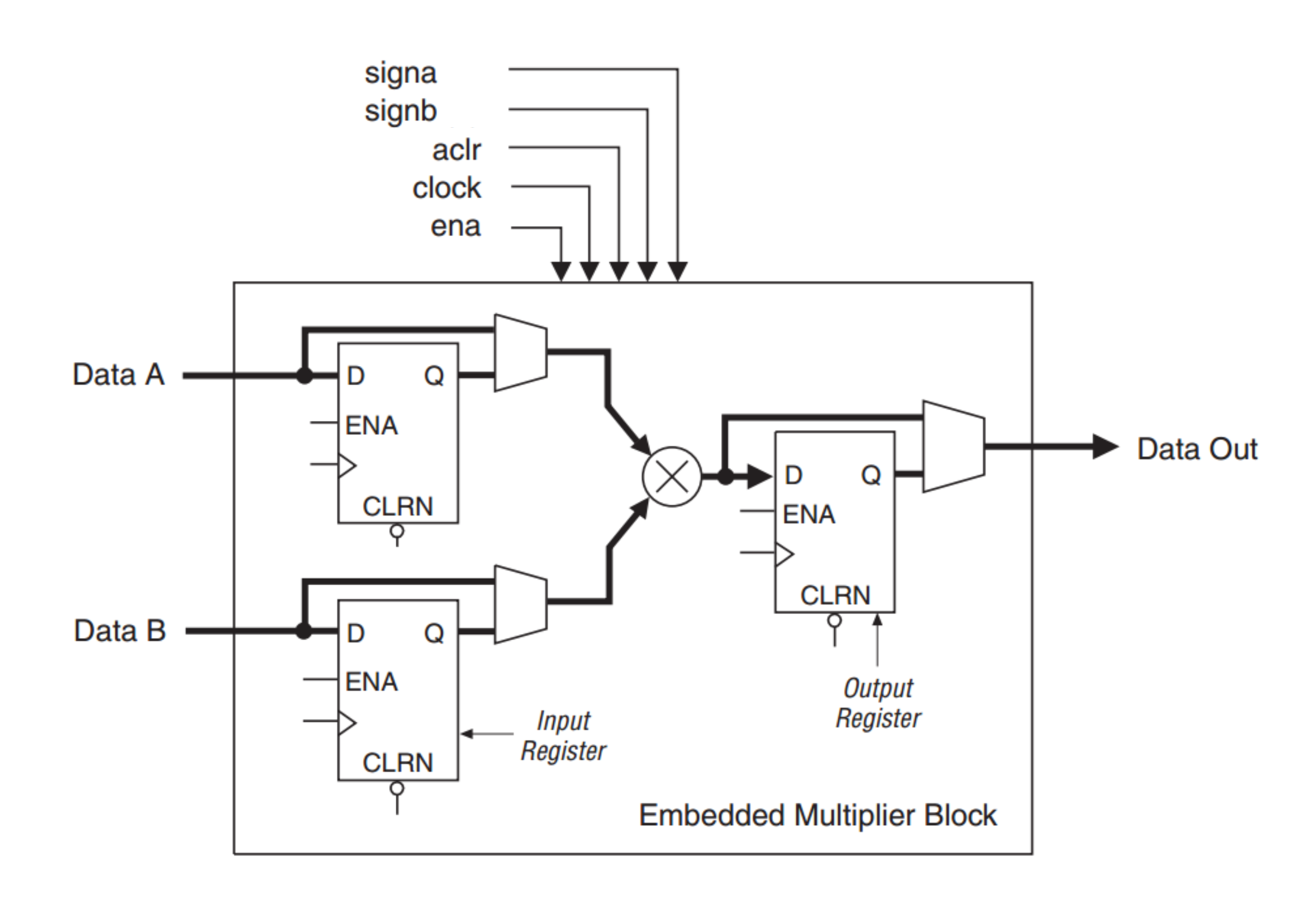
According to Figure 4, each embedded multiplier consists of the following elements: Multiplier stage, Input and output registers, and Input and output interfaces.
Embedded multipliers are arranged in columns across the device. In this way, each Cyclone II device has one to three columns of embedded multipliers. They span the height of one LAB row.
They also support:
- Signed and unsigned operations
- 18 x 18 bits and 9 x 9 bits multiplications
- Up to 250 MHz (for the fastest speed grade)
- Pipeline registers for high-performance DSP— a major step beyond the earlier FLEX 10K Series architecture that relied on configurable logic alone
Each multiplier operand can be a unique signed or unsigned number. Two signals, signa and signb, control the representation of each operand respectively. A logic 1 value on the signa signal indicates that data A is a signed number while a logic 0 value indicates an unsigned number. The sign representation of operands can be changed dynamically at run time.
2.5 Phase-Locked Loops (PLLs) and the Clock Network
Clock management is critical for high-performance synchronous systems. Cyclone II family Phase-Locked Loops (PLLs) provide general-purpose clocking with clock synthesis and phase shifting for high-speed differential I/O support.
Cyclone II family provides 16 global clock networks and up to four PLLs. The global clock network can provide clocks for all resources within the device, such as Input/Output Elements (IOEs), LEs, embedded multipliers, and embedded memory blocks. The global clock lines can also be used for other high fan-out signals.
Briefly, Cyclone II PLLs provide all-purpose clocking features:
- Clock Multiplication and Division (generating various frequencies)
- Phase Shifting and Duty Cycle Correction (for improved timing margins)
- Low-skew global clock distribution
- Regional clock networks for power efficiency
2.6 Input/Output Elements (IOEs) Structure & Features
Each Cyclone II family device’s Input-Output Element (IOE) contains a bidirectional I/O buffer and three registers (input, output, and output enable) for complete embedded bidirectional single data rate transfer. Each IOE provides buffering, programmable drive strength, register options, and various I/O standards.
In Cyclone II devices, every external pin is connected to an I/O Element (IOE) which is located around the device periphery. Each IOE serves as the interface between the FPGA’s internal logic and the external I/O pins.
Figure 5 shows the Cyclone II IOE structure.
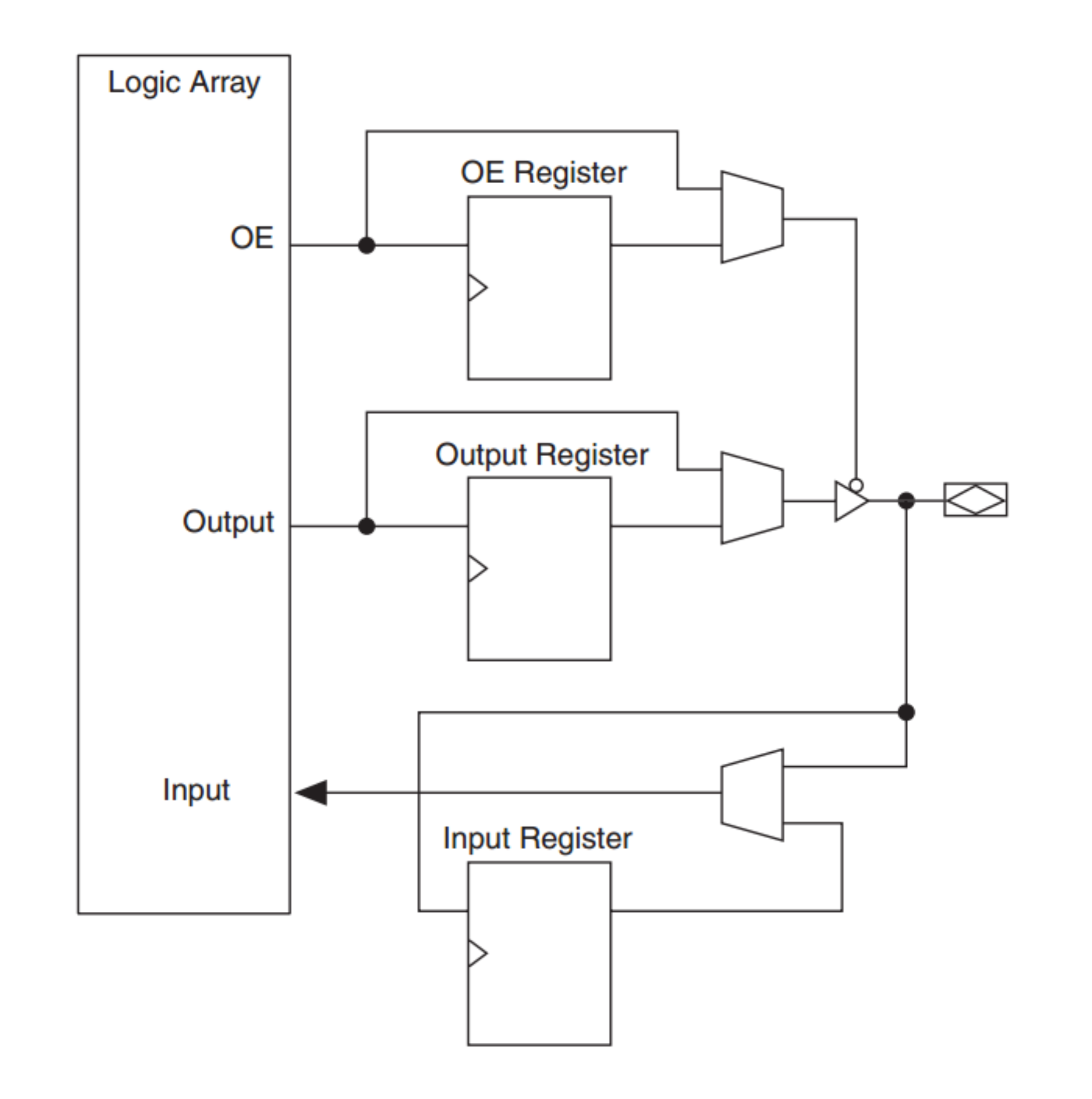
Key IOE features include:
- Support for Differential and single-ended I/O standards (e.g., LVTTL/LVCMOS).
- Peripheral Component Interconnect (PCI) compliance (3.3-V, 64- and 32-bit, 66- and 33-MHz).
- Joint Test Action Group (JTAG) boundary-scan test (BST) support.
- Programmable output drive strength, weak pull-up resistors, and bus-hold circuitry.
- Programmable input and output delays.
2.7 Interconnect Network
The Cyclone II family architecture utilizes the MultiTrack interconnect structure with DirectDrive technology. This combination makes a high-speed routing network to connect all key components: LEs, M4K memory blocks, embedded multipliers, and device I/O pins.
The MultiTrack Interconnect is a network of continuous, performance-optimized routing lines of different speeds. It can be used for inter- and intra-design block connectivity. The MultiTrack interconnect consists of row and column interconnects that span fixed distances.
DirectDrive technology actually provides a deterministic routing scheme. The same logic function will use the exact same routing resources regardless of its placement on the chip.
This structure ensures high performance and consistent, predictable results across the Cyclone II family. It also simplifies the design.
3. Overview and Key Specifications of EP2C35F484C7N FPGA
The Altera EP2C35F484C7N FPGA represents a cost-effective programmable logic device. It was introduced as part of the Cyclone II family in 2004. It was initially designed for a broad range of uses. Some of its applications include industrial control, embedded processing, communication systems, and video processing. With its specific features of 33,216 Logic Elements (LEs), a 484-pin FineLine BGA package, and 105 embedded multipliers, it offers a balanced combination of power, flexibility, and affordability.
3.1 Device Nomenclature
The EP2C35F484C7N part number clearly indicates its characteristics:
| Designator | Meaning |
| EP | Enhanced Programmable Logic Device (PLD) |
| 2 | Cyclone II series |
| C | Cyclone product line |
| 35 | Logic density (Approx. 35K logic elements) |
| F | Package type (FineLine Ball Grid Array) |
| 484 | Pin count (484 pins) |
| C | Temperature grade (Commercial: 0°C to 85°C) |
| 7 | Speed grade (Mid-range operational frequency) |
| N | Lead-free package & RoHS compliant device |
3.2 Architectural Overview of the Altera EP2C35F484C7N FPGA
Similar to the above-mentioned structure of Cyclone II family members, the core architecture of the EP2C35F484C7N FPGA has the same primary building blocks as already explained in Section 2.1:
- Logic Elements (LEs) – 33,216 total elements
- Logic Array Blocks (LABs) – 2,076 total blocks
- Embedded Memory (M4K) Blocks – 105 blocks
- Embedded Multipliers – 105 total units
- Phase-Locked Loops (PLLs) – 4 total units
- I/O Elements (IOEs) – Max 315 user I/O pins
- Global Routing Network
3.2.1 Logic Structure: Logic Array Blocks (LABs) and Logic Elements (LEs)
The EP2C35F484C7N FPGA includes approximately 33,216 total logic elements, organized into 2,076 LABs. The LEs can function as logic gates, latches/registers, counters, adders, or small Finite State Machines (FSMs). The logic elements enable the synthesis of complex logic networks inside the FPGA.
We may refer to another example of this family member with the identical structure and number of LABs.
3.2.2 Embedded Memory (M4K Blocks) Architecture
The device contains 105 embedded M4K memory blocks, each providing 4,608 bits of on-chip SRAM. The embedded memory blocks offer a total of 483,840 bits (≈ 472 Kbits).
Each M4K block features:
- True dual-port operation
- Configurable data widths (e.g., 512×8, 256×16, 128×32)
- Support for byte-enable and parity
- Built-in pipeline registers
The designers are able to configure these blocks for Synchronous/Asynchronous RAM, ROM, FIFO, or Shift Registers. Furthermore, designers can cascade multiple M4K blocks to create larger memories or distributed data buffers.
3.2.3 Embedded Multipliers and DSP Capability
The EP2C35F484C7N FPGA totally includes 105 embedded multipliers. They provide good flexibility in configuration because they can be grouped in different modes:
- 18 x 18-bit multipliers – 35 units
- 9 x 9-bit multipliers – 70 units
The architecture also allows each 18×18 multiplier to be subdivided into two 9×9 multipliers. Moreover, designers have the ability to combine multiple 18×18 multiplier blocks to implement higher-precision multiplication. They can do it manually or via synthesis tools.
These embedded multipliers, as the hardwired arithmetic units, are optimized for low latency and high throughput. In this way, they can operate up to frequencies of 200 – 250 MHz when pipelined.
This capability makes the device suitable for implementing some DSP functional modules:
- FIR (Finite Impulse Response) and IIR (Infinite Impulse Response) digital filters
- FFT (Fast Fourier Transform) and DCT (Discrete Cosine Transform) algorithms
- Matrix multipliers and correlators
3.2.4 Clock Management and Phase-Locked Loops (PLLs)
The EP2C35F484C7N includes four dedicated PLLs for on-chip clock generation and signal conditioning. The PLLs can generate clock frequencies up to 300 MHz. Of course, such a high frequency rating depends on the configuration.
Each PLL supports:
- Multiplying (×1 to ×512) or dividing (÷1 to ÷512) input clock frequencies
- Generating multiple output clocks with phase and duty-cycle control
- Reducing clock skew by using zero-delay buffering
3.2.5 EP2C35F484C7N’s I/O System and Resources
The device, in its 484-pin FBGA package, offers a maximum of 315 user I/O pins. The I/O Elements (IOEs) support a wide range of single-ended and differential I/O standards.
Each IOE Features:
- Supported I/O standards including Low-Voltage Transistor–Transistor Logic (LVTTL) and Low-Voltage Complementary Metal–Oxide–Semiconductor (LVCMOS): 3.3V, 2.5V, 1.8V, 1.5V
- Peripheral Component Interconnect (PCI) and Peripheral Component Interconnect eXtended (PCI-X) compatibility
- Support for differential signaling, including Low-Voltage Differential Signaling (LVDS), mini-LVDS, and Reduced Swing Differential Signaling (RSDS)
- Programmable drive strength (2mA to 24mA) and slew rate control
- Input and output registers for Double Data Rate (DDR) support, i.e., doubling the data throughput without increasing the clock frequency
3.2.6 Global Routing Network
Dedicated global lines run across the FPGA device , implemented as buffered networks. They can provide low-skew distribution and high fanout. These lines are separate from the general routing tracks in the FPGA device.
Global routing lines are primarily used for:
- Clock distribution: Connecting clock outputs (coming from PLLs or external pins) to registers and memory elements with minimal skew
- High-fanout control signals: Like global resetting or enabling signals
3.3 Configuration and Programming Methods in the EP2C35F484C7N FPGA
The EP2C35F484C7N is an SRAM-based device. It means its configuration is volatile and must be loaded at power-up from an external source. The device’s decompression feature allows for smaller programming file storage and faster configuration times. Therefore, it supports fast serial reconfiguration with times less than 100 ms.
This FPGA supports multiple configuration methods:
- Active Serial (AS): Using an external serial configuration device (e.g., Altera EPCS). This method is most common.
- Passive Serial (PS): Configuration data from a host processor.
- JTAG: Used for in-system debugging and initial configuration.
- Fast Passive Parallel (FPP): Used for high-speed configuration.
3.4 EP2C35F484C7N FPGA Design Tools and Development
Design development utilizes the Altera Quartus II software environment. Quartus II can run several tasks. Including that, the Quartus II software automatically infers HDL-described memory structures and maps them into the appropriate number of M4K blocks. It also selects aspect ratios and packing strategies for achieving maximum efficiency.
The Quartus II Compiler also attempts to place related logic into the same or adjacent LABs. This is to take advantage of local interconnect and register-chain routing. By applying such a method, the software can improve both performance and area utilization.
Normally, the typical design flow is:
- Design Entry: Describing hardware using HDLs (VHDL/Verilog)
- Synthesis: Translating the HDL code into a netlist of generic logic elements
- Place and Route (Fitter): Mapping the netlist onto the device’s specific resources (LEs, M4K, DSP) and determining physical wiring paths
- Timing Analysis: Verifying that the design meets timing constraints
- Compilation and Configuration: Generating the final configuration file (e.g., .sof or .pof).
3.5 EP2C35F484C7N FPGA Simulation and Verification
The Altera Quartus II can generate standard Electronic Design Interchange Format (EDIF), VHDL, or Verilog netlists.
The software also supports:
- JTAG boundary-scan testing
- Integration with third-party simulation environments such as ModelSim
- IP core integration (memory controllers, Ethernet MACs, etc.)
3.6 EP2C35F484C7N FPGA Power Consumption and Performance
The core voltage (VCCINT) is 1.2 V. The I/O voltage (VCCIO) is configurable to 1.5V, 1.8V, 2.5V, or 3.3V. The typical core current of the device is about 200 mA.
The -7 in EP2C35F484C7N denotes the speed grade. The number represents a balanced, mid-performance option.
Typical operating frequencies are design-dependent:
- Combinatorial paths: up to 250 MHz
- DSP / embedded multipliers: up to 200 MHz
- Clock distribution: up to 300 MHz (using PLLs)
Estimated power consumption values are indicated in the following table:
| Design Complexity | Clock Frequency | Estimated Power |
| Small (25% utilization) | 50 MHz | 300 – 500 mW |
| Medium (50% utilization) | 100 MHz | 600 – 1,000 mW |
| Large (75% utilization) | 150 MHz | 1,000 – 1,500 mW |
| Maximum (90%+ utilization) | 200 MHz | 1,500 – 2,500 mW |
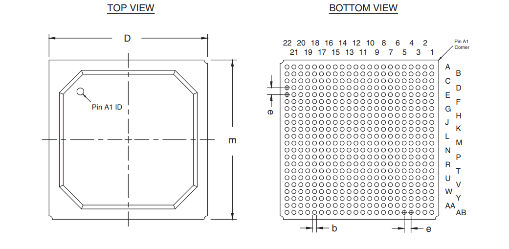
3.7 EP2C35F484C7N FPGA Packaging and Pinout
The package type is a 484-pin FineLine Ball Grid Array (BGA). The BGA packaging ensures short signal paths and low inductance for better signal integrity.
The device’s package has some characteristics:
- Pitch: 1.0 mm (standard for mid-density BGA)
- Body size: 23 mm × 23 mm
- Thermal Design Power (TDP): Low (<1.5 W typical)
- SameFrame pin-out strategy: Allows for easy PCB migration between different densities within the Cyclone II family.
Figure 6 shows a 484-pin FineLine BGA package outline. We may consider two other examples with the same packaging structure.
3.8 Key Technical Specifications of the EP2C35F484C7N FPGA
| Category | Specification |
| Logic Elements (LEs) | 33,216 |
| Total LABs | 2,076 |
| Total Embedded Memory (RAM bits) | 483,840 bits (≈ 472 Kbits) |
| M4K Memory Blocks | 105 × 4,096 bits |
| Embedded Multipliers | 35 (18×18), 70 (9×9) |
| Phase-Locked Loops (PLLs) | 4 |
| Maximum User I/O Pins | 315 |
| Core Voltage (VCCINT) | 1.2 V |
| I/O Voltage (VCCIO) | 1.5 – 3.3 V |
| Speed Grade | -7 (mid-range performance) |
| Package | 484-pin FineLine BGA |
| Typical Operating Frequency | 200 – 250 MHz |
| Configuration Modes | AS, PS, FPP, JTAG |
| Operating Temperature Range | 0°C to +85°C (Commercial) |
3.9 Applications and Advantages of EP2C35F484C7N FPGA
The EP2C35F484C7N’s excellent balance of cost, performance, and power efficiency led to its wide use.
3.9.1 Typical Applications of EP2C35F484C7N
- Data Acquisition and Control: Custom protocol handlers, high-speed data logging
- Video and Image Processing: Real-time filtering, scaling, image sensor interface logic, and format conversion
- Signal Processing: Using integrated DSP blocks
- Networking and Communications: Implementing MAC layers, packet processing, and custom interfaces
- Industrial Control and Automation: Complex state machines, motor control, PWM (Pulse Width Modulation) generation, and system monitoring
- Prototyping: Cost-effective platform for hardware prototyping of larger ASIC/SoC designs
- Education and Research Platforms: University projects, logic design coursework, and HDL training systems
3.9.2 Advantages of EP2C35F484C7N
- Cost-Effectiveness: Highly competitive price-per-LE makes the device ideal for mass-market products.
- Power Efficiency: The 90-nm process and efficient architecture contribute to relatively low static and dynamic power consumption.
- Integrated Resources: The balance of 33K LEs, 600K+ bits of memory, and dedicated multipliers reduces the need for external components and also simplifies system design.
4. Conclusion
Nowadays, the Altera EP2C35F484C7N FPGA stands as a symbol of efficient, mid-range programmable logic design. The description of mid-range refers to a group of embedded systems with 20K to 40K LE complexity.
It bridged the gap between early FPGA architectures with limited functionalities and modern FPGA systems, which feature integrated DSP blocks, hardened IP, and multi-voltage I/O.
We have already mentioned that the older generations of FPGAs, like the Altera FLEX 10K Series, simply relied on general-purpose logic and Embedded Array Blocks (EABs).
Specific features of the Altera EP2C35F484C7N made it an ideal choice for engineers seeking both versatility and performance. These features include 33,216 logic elements, 105 embedded memory blocks, and robust I/O flexibility in the FPGA architecture. These characteristics become more advantageous when combined with the Altera Quartus II toolchain.
Even decades after its introduction, this FPGA continues to serve as a valuable educational and industrial component. This product can demonstrate the enduring legacy of Altera’s engineering design philosophy: programmability without compromise!
Frequently Asked Questions (FAQ)
Q1. What are the main features of the Altera EP2C35F484C7N FPGA?
A: The device’s key features include: 33k logic elements, 483,840 bits of embedded memory, 35 hardware multipliers, 315 user I/O pins, four PLLs for clock generation, and low power consumption. Also, it supports many I/O standards, including LVDS, LVCMOS, PCI, and SSTL.
Q2. What applications use the EP2C35F484C7N FPGA?
A: Common applications can be digital signal processing (DSP), wireless communications, motor control and industrial automation, embedded controllers, and soft processors. Additionally, data acquisition and measurement systems, protocol conversion, and communication interfaces are other examples.
Q3. What is the architecture of the Cyclone II FPGA family?
A: Cyclone II family uses a hierarchical architecture built from Logic Array Blocks (LABs), Logic Elements (LEs), M4K embedded memory blocks, Embedded multipliers, Global and regional interconnect networks, Flexible I/O cells, and PLL-based clock conditioning.
Q4. How much memory does the EP2C35F484C7N provide?
A: The device contains 105 M4K memory blocks with a total of 483,840 bits of distributed on-chip RAM. These memory blocks support true dual-port operation and can be used as RAM, ROM, or FIFO structures.
Q5. Does the EP2C35F484C7N support DSP operations?
A: Yes. It features 35 embedded multipliers optimized for FIR filters, FFT operations, Convolution function, Digital modulation, and Matrix computations.
Q6. What development tools are used for the EP2C35F484C7N?
A: The primary software tool is Altera Quartus II, which supports: HDL synthesis (VHDL/Verilog), Timing analysis, Simulation, Place-and-route, and Programming via USB-Blaster.
Q7. Is the Cyclone II family still supported?
A: Cyclone II is considered mature, but still widely used. Intel company provides ongoing software support through legacy Quartus versions. And the devices remain available from distributors and long-term supply vendors.