Introduction to FPGAs
Modern electronics often require custom logic that can adapt to new requirements without hardware redesign. Field Programmable Gate Arrays (FPGAs) enable this flexibility by offering reconfigurable silicon that users can reprogram after deployment.
Field Programmable Gate Arrays (FPGAs) are versatile integrated circuits that, unlike traditional logic devices, can be programmed for various purposes. Each FPGA uses an array of logic blocks that can be programmed by users to implement custom digital functions.
The primary advantage of FPGAs is their reconfigurability: users can reprogram the device multiple times simply by loading new configuration files, without replacing any hardware. For this reason, FPGAs are also used to accelerate design cycles and reduce system costs.
In the case of FPGAs, the programmed configuration is usually volatile and therefore needs to be reloaded whenever power is applied or a different functionality is required.
Using specialized software from the FPGA manufacturer, developers can create designs using graphical tools (common for smaller FPGAs) or Hardware Description Languages (HDLs).
The two dominant HDLs are VHDL (follows the standard IEEE 1076) and Verilog (follows the standard IEEE 1364). Both allow hardware designers to describe digital circuits in a vendor-independent manner.
This vendor independence makes HDL designs portable across different FPGA platforms and reusable across projects, significantly reducing development time.
Since FPGAs use SRAM-based storage for their configuration, the programmed design is volatile and must be reloaded each time power is applied. This differs from non-volatile technologies but provides the flexibility that makes FPGAs attractive.

Historical Significance of the Altera FLEX 10K Series FPGA
Released in the mid-1990s, the FLEX 10K series was Altera’s first embedded Programmable Logic Device (PLD) and represented a major advancement in FPGA technology. It offered designers a flexible, reconfigurable platform for implementing custom digital logic circuits. Altera company is a part of Intel now.
The Flexible Logic Element MatriX (FLEX) architecture, based on reconfigurable CMOS SRAM elements, incorporated support for common pre-designed functions like adders, multipliers, and memory blocks (called ‘Megafunctions’).
The FLEX 10K family provided the density, speed, and features to integrate entire systems into a single device. Therefore, the FLEX 10K family achieved widespread adoption in the 1990s-2000s as high-density devices.
Architecture Highlights of the Altera FLEX 10K FPGA
Dual-Array Architecture
Essentially, the FLEX 10K architecture uses a dual-array structure which separates the chip into two complementary regions. Each FLEX 10K device contains an “embedded array” to implement memory and specialized logic functions, and a “logic array” to implement general logic.
Embedded gate arrays have dedicated die areas (the silicon chip area before packaging) for implementing specialized functions. By implementing functions in dedicated silicon, embedded arrays reduce die area and increase speed compared to standard gate arrays.
The embedded array is used to implement a variety of memory functions or complex logic functions, such as digital signal processing (DSP), microcontroller, wide-data-path manipulation, and data-transformation functions.
The logic array is used to implement general logic, such as counters, adders, state machines, and multiplexers. The combination of embedded and logic arrays provided the high performance and high density of embedded gate arrays, enabling designers to implement an entire system on a single device, i.e., the System-on-Chip (SoC) concept.
Configuration, In-System Programmability, and Testing Capabilities
FLEX 10K devices are programmable on the board for the specific functionality required, providing the designer the facility of iterative design changes during debugging. FLEX 10K devices are configured at system power-up with data stored in an Altera serial configuration device or provided by a system controller.
The JTAG (Joint Test Action Group) interface, standardized as IEEE 1149.1-1990, enables in-system programming of FLEX 10K devices through a serial boundary-scan mechanism. This non-intrusive testing and programming capability is built directly into the silicon.
Configuration can be loaded from system RAM, external storage, or Altera’s dedicated download cables (serial BitBlaster or parallel ByteBlaster).
As a result, this flexible interface allows microprocessors to configure FLEX 10K devices using various modes—serial or parallel, synchronous or asynchronous—depending on system requirements. Alternatively, microprocessors can treat the FLEX 10K as a memory device, loading new configurations by writing to specific memory addresses—a straightforward approach that simplifies system integration.
After a FLEX 10K device has been configured, it can be reconfigured in-circuit by resetting the device and loading new data. This in-circuit reconfiguration capability enables comprehensive device testing prior to shipment.
Figure 1 shows a block diagram of the FLEX 10K architecture.
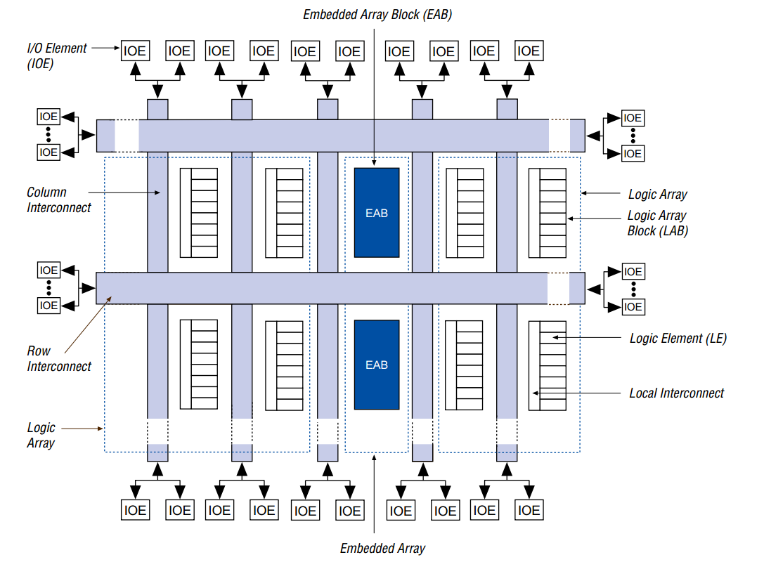
Figure 1: Altera FLEX 10K FPGA architecture block diagram
Logic Elements in the FLEX 10K Series Architecture
The Logic Array (LA) implements general-purpose logic functions using a hierarchical structure: multiple Logic Array Blocks (LABs), each containing 8 Logic Elements (LEs).
Each Logic Element (LE) contains:
- A 4-input Look-Up Table (LUT) for implementing combinational logic
- A programmable Flip-Flop with synchronous enable
- Carry and cascade chains for efficient arithmetic operations and wide logic functions
The logic element (LE) as the smallest unit of logic in the FLEX 10K architecture, has a compact size that provides efficient logic utilization. Each LUT is actually a lookup table that stores truth table values for any combinational function of up to four variables.
Therefore, each LE produces two independent outputs: one feeding the LAB’s local interconnect (for nearby LEs) and one feeding the FastTrack global routing (for remote connections – the light blue paths in Figure 1). This dual-output design certainly ensures that logic placement decisions don’t bottleneck routing resources.
Consequently, the eight logic elements (LEs) in a logic array block (LAB) can implement medium-sized logic functions individually, or multiple LABs can be interconnected to create larger blocks.
The programmable flip-flop (register) in the LE can be configured for D, T, JK, or SR types of operation. Control signals (clock, clear, preset) can come from multiple sources: dedicated global clock lines, I/O pins, or LUT outputs from any LAB.
Additionally, for purely combinational logic (functions without sequential elements), the flip-flop can be bypassed, allowing LUT outputs to feed the interconnect directly. This saves the flip-flop for sequential logic in other LEs and reduces latency.
Fast-path channels of Logic Elements in the FLEX 10K Series
Moreover, the FLEX 10K provides two dedicated fast-path channels that bypass the general interconnect, enabling efficient arithmetic and wide logic: carry chains and cascade chains:
- Carry Chains: Direct connections between adjacent LEs specifically optimized for arithmetic operations (adders, subtractors, comparators, counters). They propagate carry signals with minimal delay.
- Cascade Chains: Direct connections enabling high-fan-in logic functions (functions combining outputs from many LEs). These reduce the logic depth and delay for complex functions.
Carry and cascade chains connect all LEs in an LAB and all LABs in the same row.
Figure 2 clearly illustrates how components (flip-flop, LUT outputs, routing options) interconnect in one LE unit.
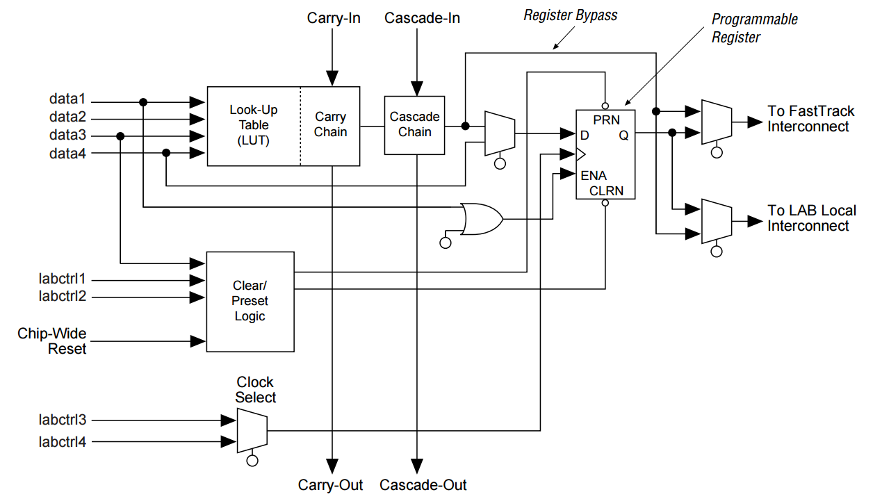
Figure 2: Logic Element block diagram in FLEX 10K FPGA
Logic Array Blocks in the FLEX 10K Series Architecture
Logic Array Blocks (LABs) provide the architectural ‘middle layer’ between individual LEs (fine-grained) and the entire chip: grouping related logic into 8-LE clusters reduces routing congestion and improves timing predictability.
In other words, each LAB groups eight LEs with four shared control infrastructure: two clock signals and two clear/preset signals, local interconnect for LE-to-LE connections, and carry/cascade chains spanning all eight elements. See Figure 3.
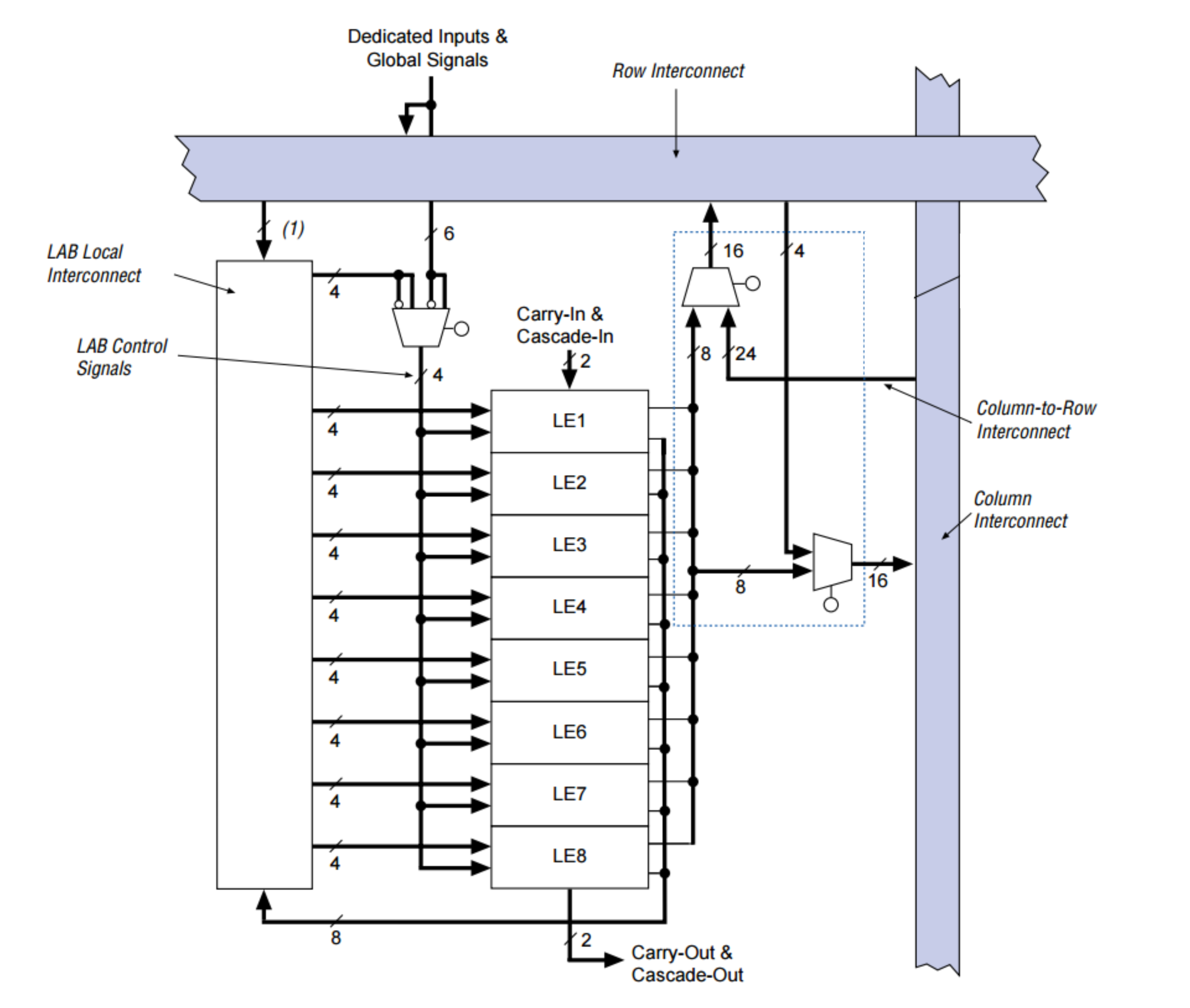
Figure 3: Logic Array Block internal structure
The LABs and EABs are interconnected by the FastTrack Interconnect (light blue paths in Figures 1 & 3).
Each LE can independently invert any of four shared control signals, allowing designers to use the same physical signal for both active-high and active-low control logic.
These can be sourced from dedicated clock pins, global routing, I/O pins, or LAB-internal logic, giving designers flexibility in how they synchronize and control state within each LAB.
The global control signals are typically used for global clock, clear, or preset signals because they provide asynchronous control with very low skew (the difference in clock arrival times) across the device.
Designers can also generate custom control signals by routing LE outputs through the LAB local interconnect—enabling conditional clocking or resets based on computed logic.
Similarly, LE outputs can drive the global control network, allowing locally-generated signals to synchronize logic across the entire device.
In summary, LABs contribute to performance because of:
- Reduced routing delay within LABs,
- Shared control signals reduce skew,
- Local interconnect faster than global routing
Embedded Array Blocks in the Altera FLEX 10K FPGA Architecture
The embedded array in the FLEX 10K architecture comprises multiple Embedded Array Blocks (EABs)—dedicated silicon blocks implementing specialized logic functions. This integration reduces die area and improves performance compared to general-purpose logic implementations.
Actually, each EAB provides 2,048 bits of embedded RAM with input/output registers, configurable as RAM, ROM, dual-port memory, or FIFO buffers. EABs can replace logic equivalent to hundreds of gates, making them ideal for implementing multipliers, microcontrollers, finite state machines (FSMs), and DSP algorithms. Multiple EABs operate independently or cascade to create larger structures.
Logic functions in the FLEX 10K FPGA can be implemented by programming the EAB with a read-only pattern during configuration, effectively creating a large look-up table (LUT). These LUT-based combinational functions operate by retrieving results instead of computing them in real time. This method offers higher performance than algorithmic implementations in general logic and is further enhanced by the fast access times of the embedded array blocks.
Moreover, all EABs within a FLEX 10K device can be cascaded to form a larger, unified RAM block of up to 2,048 words, without degrading timing performance.
Each EAB connects to the FLEX 10K interconnect matrix, receiving signals through row interconnects and driving outputs to both row and column channels. Each EAB output can drive up to two row and two column lines, while unused row channels can be driven by other logic elements (LEs). This architecture significantly enhances the routing resources and design flexibility of the device (see Figure 4).
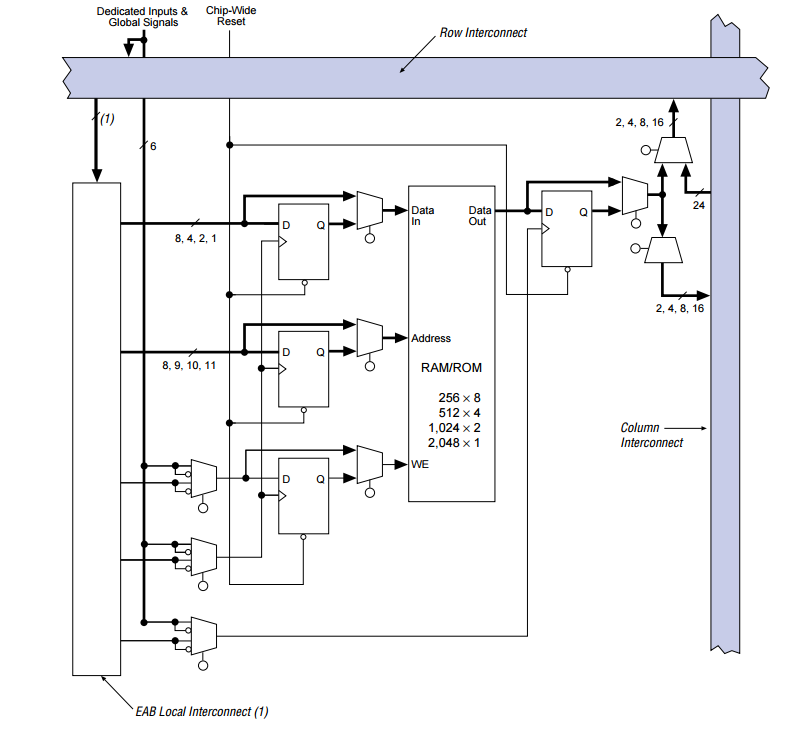
Figure 4: Embedded Array Block diagram in FLEX 10K
FastTrack Interconnect Architecture in the Altera FLEX 10K FPGA
In the Altera FLEX 10K FPGA architecture, connections between Logic Elements (LEs) and device I/O pins are established through the FastTrack Interconnect — a continuous grid of horizontal and vertical routing channels that span the entire device. This global interconnect network ensures predictable timing and performance, even in large or complex FPGA designs.
The FastTrack Interconnect is organized into row and column routing channels that extend across the entire FPGA. Each row of Logic Array Blocks (LABs) has a dedicated row interconnect, which can drive I/O pins or feed signals to other LABs. Similarly, the column interconnect transfers signals between rows and can also connect directly to I/O pins. Each I/O pin is fed by an I/O Element (IOE) located at the end of each row and column of the FastTrack network.
Each row channel can be driven either by a Logic Element (LE) or by up to three column channels. These four inputs are connected through dual 4-to-1 multiplexers, which link to two specific row channels. The multiplexer structure allows column signals to drive row channels even when all eight LEs within an LAB are actively driving the row interconnect.
Each column of LABs has its own dedicated column interconnect, which can drive I/O pins directly or connect to another row interconnect to route signals between LABs.
In summary, the FastTrack Interconnect provides a continuous routing framework that delivers fast and deterministic interconnect delays across the entire FPGA device.
Figure 5 illustrates the FastTrack Interconnect mechanism in the Altera FLEX 10K architecture.

Figure 5: FastTrack interconnect routing structure FLEX 10K
I/O Elements (IOEs) in the Altera FLEX 10K FPGA Architecture
An I/O Element (IOE) in the Altera FLEX 10K FPGA consists of a bidirectional I/O buffer and a flip-flop register that can function as either an input register—for external data requiring a short setup time—or an output register for applications that demand fast clock-to-output timing.
I/O Elements support several advanced features, including JTAG-BST (Boundary-Scan Test) capability, programmable slew-rate control, tri-state buffering, and open-drain outputs. The slew rate—the maximum rate of change of output voltage over time—defines how quickly an FPGA pin transitions between logic levels.
Importantly, by adjusting the programmable slew-rate setting, designers can optimize signal integrity or output speed based on specific application requirements.
Figure 6 illustrates the bidirectional I/O register structure within an IOE, highlighting the placement of the input/output buffers and register elements used in the FLEX 10K FPGA architecture.
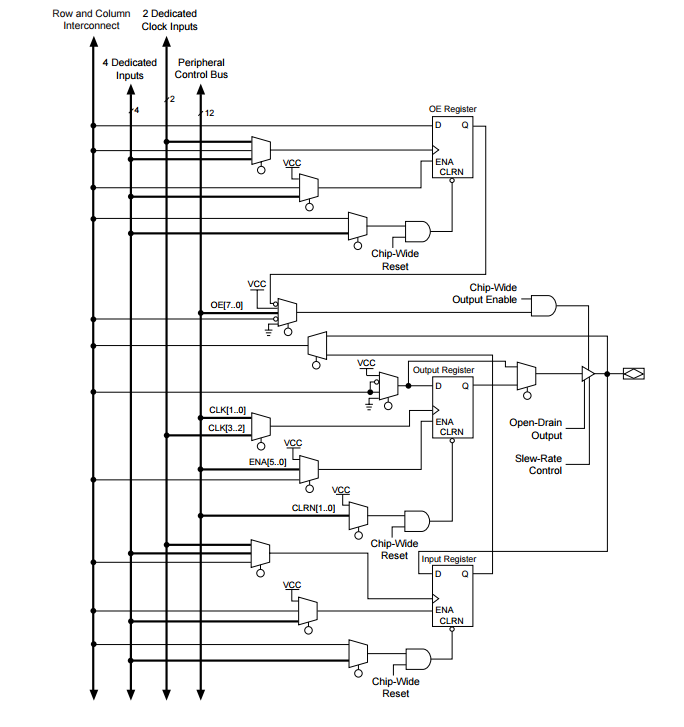
Figure 6: Bidirectional I/O element register
Each I/O Element (IOE) selects its clock, clear, clock-enable, and output-enable control signals from a high-speed distribution network known as the Peripheral Control Bus. Additionally, this bus architecture employs low-skew, high-drive buffers to ensure consistent timing and minimize signal skew across the Altera FLEX 10K FPGA device.
In addition, a Logic Element (LE) located in another row can drive a column interconnect, which in turn enables a row interconnect to propagate a peripheral control signal. A chip-wide reset signal can override all other control lines, ensuring that every IOE register is properly reset during initialization.
SameFrame Pin-Outs in the Altera FLEX 10K and 10KE FPGA Families
The Altera FLEX 10KE FPGA family supports the SameFrame Pin-Outs feature for FineLine Ball Grid Array (BGA) packages. The SameFrame Pin-Outs scheme is an Altera packaging and pin-assignment method that allows multiple FPGA devices—within the same family or closely related families—to share an identical physical pin configuration, even when their logic densities or internal architectures differ.
This capability greatly simplifies design migration and scalability, allowing engineers to design a single PCB layout and later substitute a larger or smaller device without redesigning the board.
The SameFrame Pin-Outs feature certainly defines the ball arrangement on FineLine BGA packages so that lower-pin-count packages form an exact subset of higher-pin-count configurations.
In this way, the SameFrame Pin-Outs design enables migration not only between devices of different densities within the same package, but also across package types. A single printed circuit board (PCB) can therefore support multiple FPGA density/package combinations. For instance, one board layout can accommodate devices ranging from an EPF10K10A (256-pin FineLine BGA) to an EPF10K100A (484-pin FineLine BGA) without any modification to the PCB.
Altera’s design software tools included built-in support for SameFrame Pin-Outs. Consequently, engineers could define devices for both current and future use, and the tools automatically generated pin-out files and layout guidance to help designers build PCB layouts that take full advantage of SameFrame migration capability (see Figure 7).

Figure 7: SameFrame Pin-Out example in FLEX 10K FPGA
Key Features and System-Level Capabilities of the Altera FLEX 10K FPGA Series
The FLEX 10K family introduced several advanced architectural and system-level features that enhanced flexibility, timing accuracy, and power efficiency across a broad range of digital designs.
Some of the FLEX 10K series system-level features are:
Electrical and I/O Interface:
- MultiVolt I/O interface support, enabling mixed-voltage operation across 3.3 V and 5 V systems.
- Power-efficient design, with typical standby current below 0.5 mA for most devices.
- Compliance with PCI-SIG (Peripheral Component Interconnect Special Interest Group) electrical specifications for direct PCI bus interfacing.
- Powerful I/O structure featuring:
- Individual tri-state output-enable control for each pin.
- Open-drain configuration option on all I/O pins.
- Programmable slew-rate control to reduce switching noise and improve signal integrity.
- Peripheral register for fast setup and reduced clock-to-output delay.
Clock Management and Timing:
- ClockLock and ClockBoost circuits to reduce clock-signal delay and skew while enabling clock multiplication.
- Built-in low-skew clock-distribution trees providing predictable system-level timing.
- Up to six global clock and four global clear signals for flexible timing control.
Interconnect and Logic Structure:
- FastTrack Interconnect, a continuous routing structure ensuring fast, deterministic interconnect delays.
- Dedicated carry chain for high-speed arithmetic functions (adders, counters, comparators).
- Dedicated cascade chain for implementing high-fan-in logic.
- Tri-state emulation for creating internal tri-state buses.
Test, Debug, and Reliability:
- Integrated JTAG Boundary-Scan Test (BST) circuitry available without consuming any device logic resources.
- Chip-wide reset and global-clear networks for synchronized initialization.
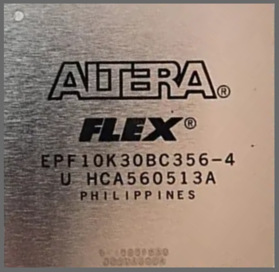
Figure 8: Top View of the Altera EPF10K30BC356-4 FPGA
Overview of EPF10K30BC356-4 FPGA
The Altera EPF10K30BC356-4, part of the FLEX 10K family, was widely deployed in embedded systems, industrial control, and telecommunications equipment throughout the late 1990s and early 2000s (see Figure 8). This legacy FPGA bridged the gap between simple Programmable Logic Devices (PLDs) and later high-density FPGA architectures.
Though now legacy, the EPF10K30BC356-4 remains available on the secondary market and represents an important milestone in FPGA evolution. Therefore, understanding its architecture illuminates how modern FPGAs evolved from these early designs.
Each component of its part number certainly reveals device characteristics:
- EPF: Denotes Altera FLEX product family designation
- 10K: Indicates FLEX 10K series
- 30: Represents approximately 30,000 (30k) usable gates
- B: Denotes the package body size designation
- C356: Specifies Ball Grid Array package (BGA) with 356 pins
- -4: Indicates the speed grade (slowest in the series)
With this nomenclature understood, let’s firstly examine the device’s specific capabilities and specifications
Key Technical Specifications of the Altera EPF10K30BC356-4 FPGA
Logic and Memory Resources
| Resource | Specification | Notes |
| Logic Elements (LEs) | 1,728 | Organized into 216 LABs |
| Logic Array Blocks (LABs) | 216 | 8 LEs per LAB |
| Usable Gates (equivalent) | ~30,000 | Typical achievable capacity |
| Maximum System Gates | 69,000 | Theoretical maximum |
| Embedded Array Blocks (EABs) | 6 blocks | 2,048 bits per block |
| Total Memory (RAM) | 12,288 bits (12 Kbits) | Configurable as various widths |
I/O Capabilities
| Parameter | Specification |
| Maximum User I/O Pins | 246 |
| Supported I/O Standards | TTL, CMOS, LVTTL |
| I/O Voltage Levels | 5V, 3.3V |
| Drive Strength | Programmable |
| Slew Rate Control | Programmable (fast/slow) |
Performance
| Resource | Specification | Notes |
| Speed Grade | -4 | slowest version in FLEX 10K series |
| Maximum Operating Frequency | 125 MHz | Design and routing dependent |
| Typical Propagation Delay | 3.5 ns | LE combinational path |
Physical Package
| Parameter | Specification |
| Package Type | FineLine Ball Grid Array (BGA) |
| Part Number Suffix | BC356 |
| Pin Count | 356 pins |
| Ball Pitch | 1.27 mm |
| Package Dimensions | 27 mm × 27 mm |
Electrical Specifications
| Parameter | Specification |
| Core Voltage (VCCINT) | 5.0V nominal (4.75V – 5.25V) |
| I/O Voltage (VCCIO) | 5.0V |
| Typical Power Consumption | 500-1500mW (application-dependent) |
Environmental Specifications
| Resource | Commercial Grade | Industrial Grade |
| Operating Temperature | 0°C to +70°C | -40°C to +85°C |
| Storage Temperature | -65°C to +150°C | -65°C to +150°C |
Design Tools and Software Support for the Altera EPF10K30BC356-4 FPGA
Configuration Sources
In fact, the device supports multiple configuration methods:
- Serial Configuration Device: External EPROM (e.g., EPC1, EPC2) provides automatic configuration at power-up
- Microprocessor/Microcontroller: Intelligent host writes configuration data to the FPGA
- JTAG Interface: Interface for in-system programming during development
- Passive Serial (PS) Mode: External controller provides configuration bitstream serially
- Passive Parallel Asynchronous (PPA) Mode: Faster parallel configuration for high-volume manufacturing
Development Softwares
Altera previously provided several tools for developing designs for the EPF10K30BC356-4 as follows:
- Altera MAX+PLUS II: It was the primary development environment when the EPF10K30BC356 was released in the late 1990s. It provided synthesis, simulation, Synthesis, timing analysis, and device configuration file generation for the FLEX 10K FPGA family. MAX+PLUS II ran on DOS, Windows, and Unix workstations. The final version (v10.2, released about 2001) remains the most reliable tool for FLEX 10K designs. Altera MAX+PLUS II later superseded by Intel Quartus II.
- Altera later introduced Quartus II in 1999 as MAX+PLUS II’s successor, with improved synthesis algorithms and a more modern interface. FLEX 10K support continued through Quartus II version 13.0 SP1 (2013), after which the devices were officially declared end-of-life. Modern Quartus Prime versions no longer support FLEX 10K devices. For engineers maintaining legacy systems, MAX+PLUS II v10.2 (the final version) and Quartus II v13.0 SP1 (the last to support FLEX 10K) remain available through Intel’s legacy download portal.
Design Entry Methods
Designers could implement projects using multiple entry styles:
- HDL-based: Designers could implement projects using Hardware Description Languages (HDLs) such as VHDL or Verilog,
- Schematic-based: Graphical logic capture using primitive gates and megafunctions
- Mixed-mode: Combination of HDL modules and schematic blocks
- State machine entry: Graphical state diagram capture with automatic HDL generation
Applications of the Altera EPF10K30BC356-4 FPGA in Embedded and Industrial Systems
During its production years (late 1990s-early 2000s), the EPF10K30BC356-4 enabled implementation of complete subsystems across diverse applications:
Digital Signal Processing (DSP):
- Digital filters (FIR, IIR)
- FFT/IFFT implementations
- Audio/video processing pipelines
- Modulation/demodulation circuits
Telecommunication Systems:
- Line coding
- Interface adaptation
- Protocol converters
- Serial-to-parallel interfaces
- Data encryption/decryption
- Error Detection and Correction (ECC)
Industrial Automation and Control:
- Real-time logic
- Motor control systems
- Process control logic
- Sensor interfaces
- Data acquisition
- Programmable Logic Controller (PLC) implementations
- Safety systems
Embedded Systems:
- Custom peripheral controllers
- Memory controllers
- System glue logic
- Bus interface adapters
Prototyping and Development:
- ASIC prototyping before fabrication
- Algorithm validation
- Hardware/software co-design
- Educational purposes
Consumer Electronics:
- Gaming Peripherals
- Set-Top Boxes
Conclusion: Historical Significance of the Altera EPF10K30BC356-4 FPGA
The Altera EPF10K30BC356-4 FPGA represents a pivotal milestone in the evolution of programmable logic technology. Released in the late 1990s as part of the FLEX 10K family, it offered digital designers a powerful platform. Although technology has advanced dramatically since its release, the core architectural principles embodied in this device—programmable logic elements, embedded memory, hierarchical routing, and flexible I/O structures—remain fundamental to today’s FPGA design philosophy.
Despite being obsolete, the EPF10K30BC356-4 remains valuable for several purposes:
- Legacy System Maintenance: Engineers supporting existing industrial or embedded systems continue to rely on this device for dependable operation and easy integration.
- Replacement and Repair: The FPGA serves as a critical replacement part in older systems where redesigning or requalification would be costly.
- Educational Use: Ideal for academic laboratories and training environments, the device enables students to learn fundamental FPGA design principles without the complexity or resource overhead of newer architectures.
- Cost-Sensitive Applications: Useful for projects that do not require modern FPGA features or high-speed logic performance.
- 5 V Logic Compatibility: Directly interfaces with legacy 5 V logic systems without requiring level shifters or external translation circuitry.
Therefore, the EPF10K30BC356-4 FPGA continues to appear in academic research labs, retro computing projects, and industrial maintenance workflows. Studying its architecture provides deep insight into the evolution of programmable logic design and the transition from early gate-array devices to the advanced FPGA platforms of today, you can also see another member of the Altera 10K family here
Frequently Asked Questions (FAQ)
A: It is a legacy programmable logic device designed for implementing custom digital circuits, such as signal processing, memory interfacing, and control systems in embedded and industrial electronics.
A: The EPF10K30BC356-4 is supported by Altera’s Max+Plus II design software, which includes simulation, place-and-route, and configuration tools.
A: No. It’s an end-of-life device, but it remains available through legacy component suppliers for maintenance and educational use.
A: The device operates at 5V core voltage and supports 3.3V or 5.0V I/O standards, making it ideal for 5V-compatible systems.
A: Altera (now Intel) replaced it with more advanced families like Cyclone and Stratix, which use modern 1.2V–3.3V logic levels and larger embedded memory blocks.