Introduction
Voltage regulation is one of the basic requirements in modern electronic systems. Maintaining a stable output voltage is critical for reliable and efficient operation in several applications such as industrial controllers, IoT devices, embedded systems, etc.
Power supplies do not provide perfectly regulated voltages. Fluctuations in the output voltage can damage the sensitive components or degrade the performance. Thus, to maintain the stable voltage, voltage regulators play an essential role. Among the most commonly used regulators are Low Dropout Regulators (LDOs) and buck converters (switching regulators).
Selecting between an LDO and buck converter is not a straightforward task. Each of them holds different advantages and trade-offs in terms of cost, complexity, efficiency and noise. Therefore, understanding these parameters is essential for designing efficient power systems.
This comprehensive guide will provide a deep dive into the LDO vs buck converter comparison. The focus will be on working principles, efficiency and noise characteristics for both devices. In addition, a real-world case studies will be provided to help engineers select the optimal solution for the specific application.
What is a Low Dropout Regulator (LDO)?
Fundamentally, a Low Dropout Regulator (LDO) is linear voltage regulator that works by dissipating voltage as heat providing a simple and low-noise solution. Particularly, LDO is designed to operate even when the input voltage is very close to the desired output voltage hence the name low dropout.
Working Principle of an LDO
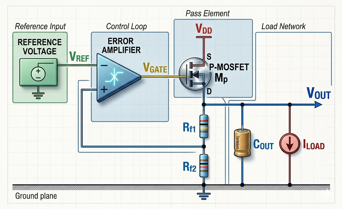
An LDO functions as a variable resistor. As shown in Fig-1, it utilizes a closed-loop control system consisting of an error amplifier, a voltage reference, and a pass element, typically a N-channel or P-channel MOSFET (e.g., TPS7A4701 series).
The function of the error amplifier is to compare the feedback voltage from the output with an internal reference voltage. Based on the comparison, it adjusts the gate driver of the transistor, varying the resistance to uphold a stable output voltage, irrespective of load transients or input fluctuations.
Key Characteristics
- Widely used in low-noise and precision applications, with devices such as the TPS7A4701 series commonly used in high-performance designs
- Fast transient response
- Simple design utilizing lower external components
- Lower efficiency if input-output voltage difference is large
Advantages and Disadvantages of an LDO
Following table presents the advantages and limitations of a conventional LDO.
| Advantages | Disadvantages |
| Low ripple and noise | Efficiency decreases as the input-output voltage difference increases, leading to higher power dissipation |
| Easy to design and implement | Excessive heat generation due to power dissipation |
| No switching components hence no EMI issues | Not suitable for high current applications |
What is Buck Converter?
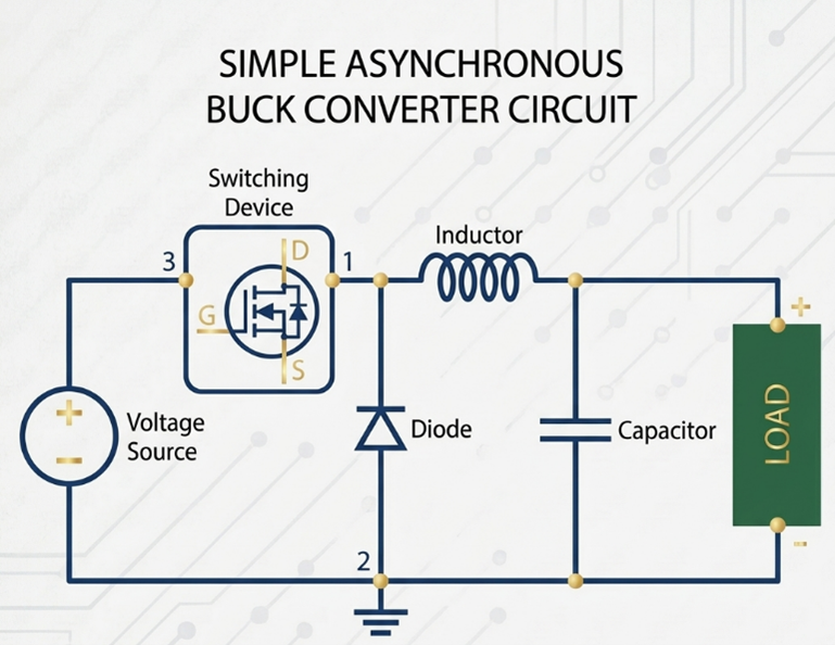
A buck converter, also known as step-down converter, is type of switching regulator that efficiently reduces voltage using high-frequency switching elements. Unlike an LDO, a buck converter operates by switching a transistor such as MOSFET, IGBT, etc. fully on and fully off (further details here).
Buck converters can be broadly classified into synchronous and asynchronous types. In synchronous designs, the diode is replaced with a second controlled switch, improving efficiency, especially at higher currents. However, for regulator selection purposes, both types follow the same fundamental operating principle and trade-offs.
Working Principle of Buck Converter
As depicted in Fig-2, buck converter consists of a switching element (MOSFET/IGBT), a diode (sometimes a second MOSFET/IGBT), an inductor, and an output capacitor.
When the primary switch is closed (while the other switch remains open), the current flow from input supply, storing energy in the inductor’s magnetic field and supplying it to the load.
When the primary switch is open (closing second switch/diode), the stored energy in the inductor is released to the load through the second switch/diode. The turn-on and turn-off of the switch are controlled by the gate signal. The buck converter maintains the stable output voltage by controlling the duty cycle (ratio of turn on time to total period). Mathematically, the duty cycle is given as:
\[D = \frac{V_{OUT}}{V_{IN}}\]
Key Characteristics
- Suitable for higher current applications
- Offers higher efficiency (85-95%)
- Complex than LDO
Advantages and Disadvantages of a Buck Converter
Following table presents the advantages and limitations of a conventional buck converter.
| Advantages | Disadvantages |
| Higher efficiency even at larger voltage difference | Due to switching element, higher ripple and EMI issues |
| Lower heat generation | Requires extra care during PCB layout |
| Suitable for high power applications | EMI considerations |
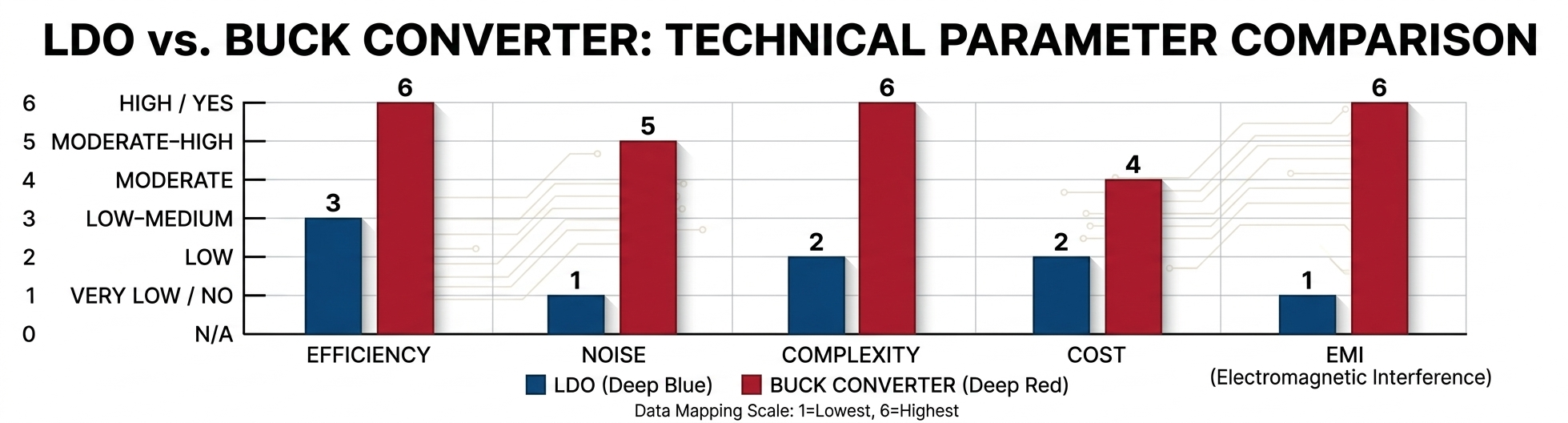
LDO vs Buck Converter: Efficiency vs Noise
The efficiency of an LDO can be estimated using a simple relation:
\[\eta_{LDO} = \frac{V_{OUT}}{V_{IN}}\]
This indicates that efficiency is directly dependent on the ratio of output to input voltage. A large voltage difference results in poor efficiency.
In contrast, the efficiency of a buck converter is influenced by conduction and switching losses and can be approximated as:
\[\eta_{Buck} = \frac{P_{OUT}}{P_{OUT} + P_{Loss}}\]
where losses include switching losses, conduction losses, and parasitic effects.
To understand which one is better for specific application, it is important to analyse how each of them handle the most critical parameters: efficiency and noise. The table below demonstrates efficiency comparison for both devices.
| Feature | LDO | Buck converter |
| Driving Efficiency | Depends heavily on input and output ratio | Consistently high across various input ranges |
| Heat generation | High | Low-moderate |
| Light load efficiency | Excellent (performs better if input voltage is close to desired voltage) | Can drop off |
| Max efficiency | Variable (30-90% depends on voltage difference) | 85-95% |
LDO vs Buck Converter: Efficiency Trap
Assuming it is required to drop down 12V battery voltage to 3.3V to draw a 1A of current. In this scenario, if LDO is used, it must dissipate 8.7W of power as heat ((12V – 3.3V)×1A]). This will instantly destroy a standard surface mounted (SMD) component. Consequently, in this case, buck converter will be preferred choice.
On the other hand, if drop down is required from 3.3V to 2.8V at 100mA, the power dissipation in LDO will be only 0.05W. Hence, in this case, LDO will be preferred choice.
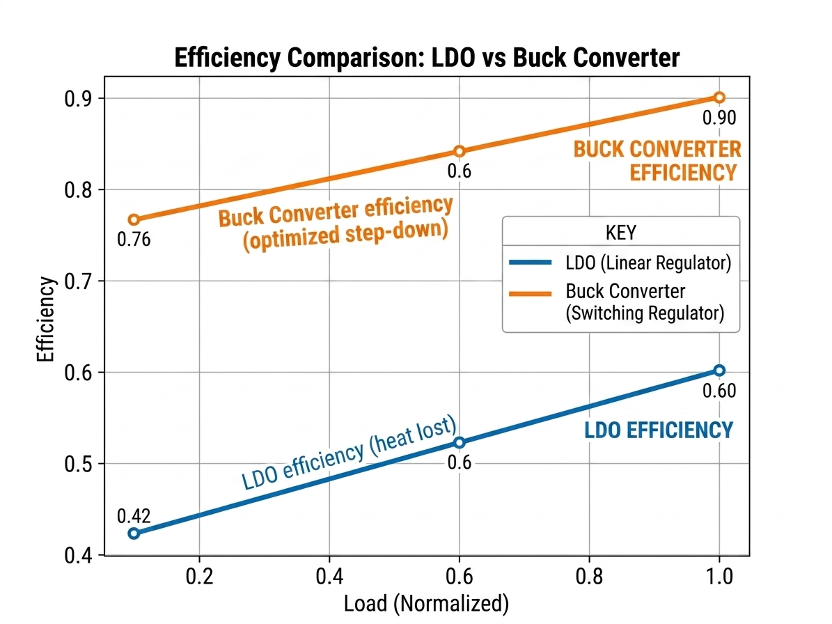
This concept is further demonstrated in Fig. 3, where the efficiency of an LDO (blue) remains limited due to its linear operation, while the buck converter maintains higher efficiency (orange) across a wide load range. This difference becomes more significant at higher load currents, making buck converters more suitable for power-intensive applications.
LDO vs Buck Converter: Noise and Ripple
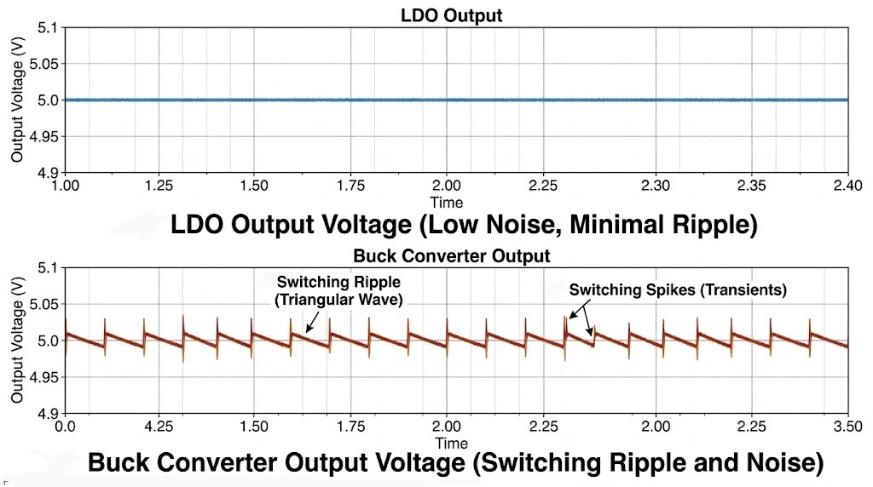
Although buck converters excel in efficiency, their switching nature inherently introduces noise challenges. The switching node transitions at a very high frequency (typically 100kHz and higher), generating a square waveform with significant harmonics. As shown in Fig-4, these harmonics result in output voltage ripple and EMI issues, which may degrade the performance of noise-sensitive system.
The output voltage ripple in a buck converter can be approximated as:
\[\Delta V = \frac{I_{OUT} \times (1 – D)}{f_{SW} \times C}\]
where D is the duty cycle, fSW is the switching frequency, and C is the output capacitance. This relationship shows that higher switching frequency and larger capacitance reduce output ripple.
Conversely, LDO regulators provide low noise operation owing to their linear topology. Without high-frequency switching, the switching ripple and EMIs are significantly reduced.
Another important parameter in LDO performance is Power Supply Rejection Ratio (PSRR), which indicates how effectively input voltage noise is suppressed at the output. While PSRR varies with frequency, LDOs generally provide excellent noise rejection at lower frequencies, making them suitable for precision analog applications such as analog to digital converter (ADCs), precision sensors, and RF transceivers..
LDO vs Buck Converter: Summary Comparison
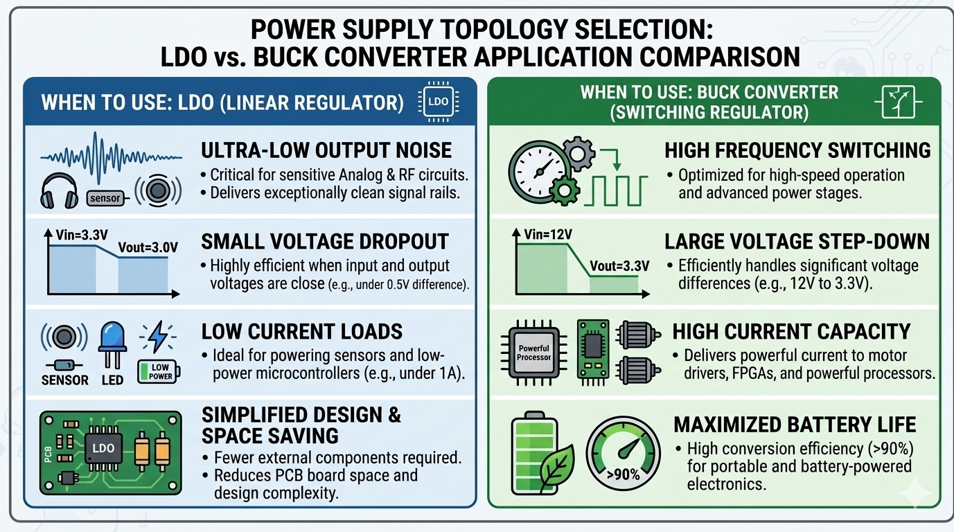
LDO vs Buck Converter: When to Choose What?
| Use LDO When | Use Buck Converter When |
| Low noise is critical | High frequency is required |
| Small voltage difference | Large voltage drop exists |
| Low current applications | High current systems |
| Simplicity is preferred | Battery life is important |
LDO vs Buck Converter: Case Studies
In this section, three different case studies are explored and the most suitable regulator for each scenario is selected based on the given requirements.
Case Study 1: Powering a High Resolution 24-bit ADC
Requirement:
An engineer needs to design a medical device that measures very low level (micro-volt level) voltage utilizing a precision 24-bit ADC. The input supply is 5V and the ADC requires a 3.3V supply.
Solution:
If a buck converter is used in this scenario, the 10 mV–30 mV switching ripple could easily overwhelm the microvolt-level signal that the ADC is designed to measure. In contrast, considering PSRR, an LDO offers the 5 V rail to be regulated cleanly, further ensuring a stable and noise-free supply for the specified application (e.g., TPS7A9401).
Case Study 2: 12V Automotive System to 5V Microcontroller
Requirement:
An automotive system needs to power a 5V microcontroller from a car battery that fluctuates between 12V-14V. The microcontroller draws a current of 1.5A.
Solution:
Selecting LDO in this scenario would result in a thermal bottleneck. Stepping down from 14V to 5V at 1.5A leads to power dissipation of 13.5 W, which is excessively high and can overheat or damage the device.
Conversely, A buck converter efficiently handles this large voltage drop, maintaining efficiency greater than 90% while significantly reducing heat generation and extending battery life.
Case Study 3: The Hybrid Approach
Requirement:
An IoT wireless sensor requires a 3.3V supply of its RF transceiver drawing a current of 300mA. The power source is 9V battery. It is worth noting that RF circuit is highly sensitive to noise which can directly impact signal integrity and communication range.
Solution:
The most effective solution in this scenario is a hybrid power architecture, combining buck converter followed by an LDO regulator.
Using LDO alone for such conversion from 9V to 3.3V would result in significant power loss (1.71W as heat). This not only reduces efficiency but also creates thermal challenges, especially in compact IoT designs.
On the other hand, using buck converter alone to directly powering RF circuit would introduce severe noise and ripple. This noise can degrade RF performance, reduce signal quality, and ultimately limit the wireless communication range.
A hybrid approach could address both challenges effectively. A buck converter first steps down the voltage from 9V to 3.6V with high efficiency. Later, an LDO regulator further reduces that voltage from 3.6V to 3.3V. Since the voltage drop is too small, the resulting power dissipation is minimal (0.09W).
LDO vs Buck Converter:Layout and Thermal Management Considerations
Even after an appropriate choice of topology, a poor PCB layout can destroy power supply. This section demonstrates how proper PCB layout and thermal management is important for both regulators.
Buck Converters
For buck converter, the most critical layout consideration is minimizing high frequency loops, often referred to as hot spots. These loops involve input capacitor, MOSFET (Also read our MOSFET selection guide), and the return path. The components must be placed as close as possible to shorten these loops, leading to reduction in parasitic inductances.
Poor layout in this region can result in significant voltage spikes, higher switching losses, and severe EMI, ultimately degrading overall system performance.
LDOs
LDOs have simple layout requirements, however thermal management becomes the primary concern. Since LDOs dissipate significant heat, the PCB itself acts as an effective heatsink (Read our article on power dissipation and thermal management in LDOs). This can be achieved by using wider copper pours connected to the LDO ’s thermal pad, along with multiple thermal vias tied to the ground plane. Proper heat distribution ensures that power loss is efficiently dissipated.
LDO vs Buck Converter: Common Design Pitfalls
- Overlooking efficiency in high voltage drop applications
- Ignoring noise requirements in sensitive circuits
- Understanding thermal dissipation
- Choosing complexity over simplicity
Practical Applications of LDOs and Buck Converters
| LDO | Buck converter |
| Analog to Digital Converter (ADC) | Microcontroller Unit (MCU) |
| Digital to Analog Converter (DAC) | Field Programmable Gate Array (FPGA) |
| RF amplifier | LED driver |
Recent Trends in Voltage Regulators
Modern power electronics is evolving rapidly, and voltage regulators, such as LDOs and buck converters have seen significant improvements in recent years.
One of the key advancements in buck converters is the introduction of low-EMI designs. These converters use spread-spectrum switching and optimized layouts to reduce EMI, making them suitable for noise-sensitive systems.
In addition, wide bandgap devices (WBG) such as Gallium Nitride (GaN) and Silicon Carbide (SiC) are enabling higher switching frequencies and improved efficiency, allowing designers to shrink the size of passive components and increase power density.
On the other hand, ultra-low quiescent current (IQ) LDO regulators are becoming increasingly popular especially in battery-powered applications. Such devices consume minimal current during standby, significantly enhancing battery life in IoT and wearable systems.
These advancements provide engineers with more flexibility in selecting the appropriate regulator while balancing efficiency, noise, and system complexity.
Conclusion
Selecting between an LDO and buck converter needs a clear understanding of system requirements. LDOs offer simplicity and low noise, however they suffer from poor efficiency when the voltage difference is large. In contrast, buck converters provide high efficiency and better thermal performance but introduce complexity and noise in the system.
In real-world applications, engineers can also apply a hybrid approach by using buck converter and LDO together to provide high efficiency and low noise signal to specific application. Ultimately, the final choice depends on balancing efficiency, noise, cost and design complexity.
Frequently Asked Questions (FAQs)
The dropout voltage is the minimum required difference between the input voltage and the output voltage for the LDO to maintain regulation. For example, if an LDO is set to output 3.3V and has a dropout voltage of 200mV, the input voltage must be at least 3.5V. If the input drops below 3.5V, the output will “drop out” of regulation and follow the input down.
No. A buck converter is strictly a step-down regulator. To step a lower voltage up to a higher voltage, you must use a Boost Converter topology. If your input voltage fluctuates both above and below your desired output, a buck-boost converter is required.
Audible noise in a buck converter is typically caused by piezoelectric effects in ceramic output capacitors or magnetostriction in the inductor. This usually happens when the converter enters Pulse-Skip or light-load modes, dropping its switching frequency down into the human audible range 20Hz to 20kHz.
It depends on the sleep state. If the device spends 99% of its time in deep sleep drawing microamps, an LDO with an ultra-low quiescent current (IQ) is often superior, as buck converters require power just to run their internal switching oscillators. However, if the device transmits frequently, a buck converter will drastically extend battery life during active periods.
Power Supply Rejection Ratio (PSRR) measures an LDO’s ability to reject noise from the input supply and prevent it from passing through to the output. It is measured in decibels (dB). A high PSRR (e.g., 70dB at 1kHz) indicates excellent noise filtering capabilities.
COMMENTS