Introduction
Many electronic devices, such as battery chargers, microprocessors, desktop PCs, RISC processors, and embedded systems, require stable, low-voltage power and draw more current. The LT1085 LDO is designed to handle up to 3A with 1V dropout, and it is frequently desktop PCs, RISC processors, and embedded systems.
The LT1085 is a positive adjustable low-dropout linear voltage regulator with upto 3A of output current handling capability. It has a wide input voltage range of 2.5V to 30V. The output voltage is adjusted by choosing the appropriate external resistor value. This LDO comes in a simple 3-pin configuration, i.e., input, output, and one adjustment pin. The LT1085 falls under the linear voltage regulators, which means it dissipates excess voltage between the input and output directly as heat. Therefore, in applications that require high current, LT1085 can quickly overheat; therefore, proper heat sinking is essential in such designs.
This technical tutorial will cover the LT1085 pinout, it’s typical circuit design, technical specifications, design considrations, thermal design calculations, and 5V/3A power supply design with LT1085 voltage regulator.
What is LT1085 LDO?
LT1085 is the Low Dropout voltage regulator that maintains a constant output voltage regardless of the variations at the input side. It has a wide input voltage range between 2.55V and 30V and consists of only three pins, known as input, output, and one adjustment pin for choosing the desired output voltage. LT1085 comes in many versions offering different output current ratings. For example, LT1083 offers 7.5A output current, LT1084 offers 5A output current, and LT1085 can deliver 3A of continuous current for driving the output loads such as battery chargers, desktop PCs, and constant current regulators.
Unlike other LDOs, LT1085 is known for its high current-delivering capability, which is up to 3A. LT1085 can maintain voltage regulation with a very small voltage difference between input and output, which is not possible with regulators like LM317 and IC 7805.
The LT1085 is available in fixed-output (3.3V, 5V, 12V) and adjustable-output versions, giving designers flexibility across a wide range of voltage requirements. Its simple design, high efficiency, and current handling capability, and minimum external components requirement make it suitable for a range of applications including battery chargers, post regulators, switching supplies, and embedded systems.

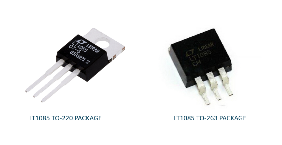
LT1085 Pinout and Typical Packages
The LT1085 has a very simple pin configuration (input pin, output pin, and adj pin) and requires only two external resistors for output voltage adjustment. It comes in various packages, but the most common ones are T0-220 and TO-263 (D²PAK). Understanding the pinout and package options is essential for correct schematic design, PCB layout, and thermal planning.

LT1085 Pinout Function
Each pin of the LT1085 LDO serves a unique function, and correctly using them in the design is essential for the proper functioning and operation of the desired circuit. The table below illustrates the proper pin numbering along with its function.
LT1085 Pin Function Description
LT1085 Typical Packages
Choosing the right package for your LDO is essential because it directly impacts the thermal performance of the device, especially in high-current applications. All the LT1085 regulators share the same pinout, but the physical form factor of the device varies depending on the selected package type.
Typical LT1085 Packages and Their Use Cases
Technical Specifications and Parameters of LT1085 LDO
Most designers often only consider the input and output voltage requirements of the design and overlook the key design parameters, which leads to design failure. Understanding the technical specifications of the LT1085 LDO regulator is essential for designing reliable and efficient circuits. These specifications not only define the device’s electrical limits but also directly influence thermal design, power dissipation, and real-world application suitability.
Key Design Parameters of LT1085 LDO
Key Electrical Parameters of LT1085 LDO
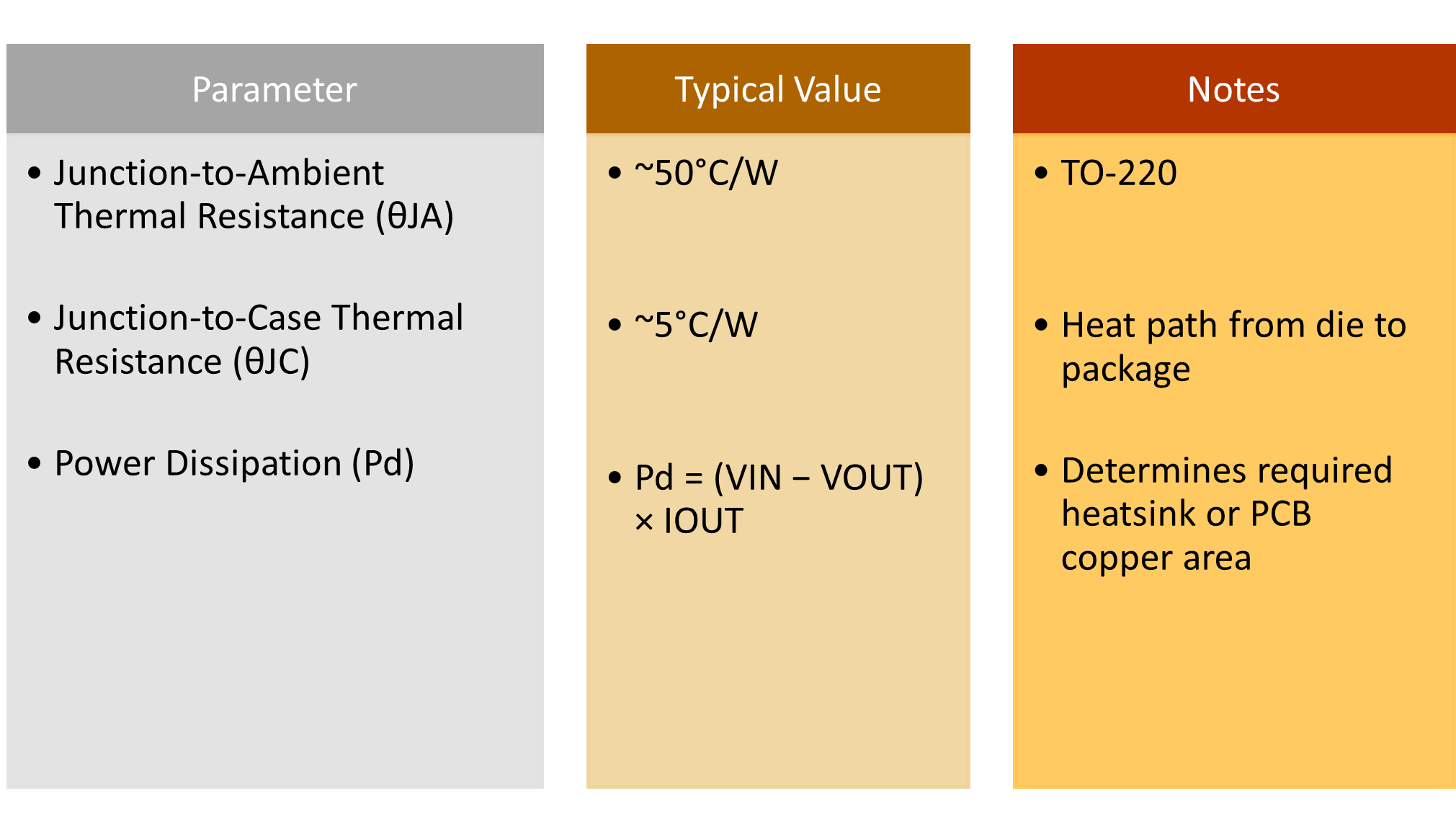
Thermal Parameters
From the datasheet of LT1085, note the Junction-to-Ambient Thermal Resistance (θJA) and Junction-to-Case Thermal Resistance (θJC). Now, calculate the power dissapation using;
PD = (VIN − VOUT) × IOUT
Using these parameters, one can design the required heat sink for their specific application, which is discussed in detail in the thermal design calculation section of this article.
Absolute Maximum Ratings
The absolute maximum ratings are as important as key technical specifications because they tell the designers the maximum operating limits of the device. Operating beyond these limit make the device to fail or burn instantly.
LT1085 Maximum Ratings
Power Dissipation in the LT1085
Power dissipation is one of the most crucial factors that can impact the performance and reliability of the device. LT1085 belongs to the linear voltage regulators and thus dissipates the excess voltage as heat; therefore, power loss increases with both voltage drop and load current, making thermal management essential in all high-current designs.
The power dissipated by the LT1085 is calculated as:
PD = (VIN − VOUT) × IOUT
For example, in a certain design, the input voltage of the LDO is 9V, the output voltage is 5V, and the load current is 3A. In such a case, the power dissipation by the LT1085 will be;
This 12W of heat must be removed efficiently via a heatsink or PCB thermal design. Otherwise, the regulator will enter thermal shutdown.
Thermal Design and Junction Temperature Calculation
The LT1085 LDO regulator can deliver up to 3A of continuous current, but as a linear regulator, any voltage difference between the input and output is dissipated as heat. Therefore, proper thermal design is critical to prevent overheating, thermal shutdown, and long-term reliability issues.
Calculate Power Dissipation
The power dissipation calculations are already discussed in the above section. Power dissipation is the starting point for any thermal design. For a specific design application, if the input voltage is 9V and the output votlage is 5V, and the current requirements are continuous 3A. In such a case, the power dissipation will be;
This 12 watts of power must be safely removed in the form of heat to keep the junction temperature below the 150°C thermal shutdown limit.
Determine Maximum Junction Temperature
The junction temperature depends on ambient conditions. Note down these specifications from the LT1085 datasheet to find the maximum junction temperature.
Junction Temperature Equation
TJ = Junction temperature
TA = Ambient temperature
PD = Power dissipation
θJA = Thermal resistance, junction-to-ambient
If no heat sink is used, then the junction temperature for 12 watts of power dissipation will be;
Calculate Required Heatsink Thermal Resistance
The total thermal resistance from junction to ambient must satisfy:
If we take the maximum junction temperature 125°C (safe margin below 150°C), and 12 watt power, then the junction to ambient resistance will be;
When designing a high-current LT1085 LDO circuit, the total thermal resistance from the junctionto the ambient air determines whether the device will operate safely. The thermal path is composed of three main parts, which are;
θJC = Junction-to-Case thermal resistance (from IC die to package)
θCS = Case-to-Heatsink thermal resistance (interface material)
θSA = Heatsink-to-Ambient thermal resistance (through air or convection)
θJA(total) is the sum of these resistances, representing the total thermal path from junction to ambient.
We have already calculated the θJA(total). Now, only plug all the values to get the heat sink to ambient thermal resistance θSA.
This shows that we need to use heatsinks with θSA ≤ 0.75°C/W for high-current applications.
Circuit Design with LT1085 LDO
Designing a circuit with the LT1085 LDO regulator requires careful attention to input voltage, output voltage selection, load current, thermal management, and stability components. A properly designed LT1085 circuit delivers clean, low-noise, and reliable power, making it ideal for applications such as industrial control systems, embedded devices, audio amplifiers, and linear power supplies.
Choose the Input and Output Voltages
Depending upon your application, select the desired input and output votlage of LT1085. But, keep in mind that the input voltage must be higher then the desired output voltage by atleast the dropout voltage, which is typically 1.3V for LT1085 LDO. For example, for a 5V output at 3A, VIN should be ≥ 6.5V to maintain regulation.
The output voltage is fixed using the two external resistor divider network for the ADJ pin.
Select Output Resistors
The LT1085 uses an external resistor divider (R1 and R2) connected between the output pin, ADJ pin, and ground to precisely set the output voltage. Internally, the regulator maintains a constant reference voltage (VREF) of 1.25V between the OUT and ADJ pins. T
Therefore, keeping the VREF equal to 1.25V, and Vout 5V, and by choosing the R1, we can find the value of R2. If we choose R1 to be 240 ohms, then R2 will be 720 ohms. The formula used to calculate the value of R2 is;
Input and Output Capacitors
Proper input and output capacitor selection is critical to ensure stability, noise suppression, and fast transient response when designing a power supply with the LT1085 LDO. Unlike switching regulators, LDOs rely heavily on external capacitors to maintain stability and to handle sudden load or input voltage changes.
Input Capacitor
According to the datasheet of LT1085, a 10µF electrolytic capacitor should be connected between the input and GND. When designing the PCB layout, ensure that the capacitor is placed close to the VCC pin and GND of the LT1085 IC. This will filter input voltage ripples and noise and prevent oscillations caused by input impedance. To use the LT1085 in your Altium or KiCad designs, you can download its symbol and footprint from the files listed below.
Output Capacitor
Similarly, according to the datasheet, it is recommended to place the 10µF electrolytic capacitor between the output pin and ground. Also, place this capacitor very close to the output pin and GND to reduce the output voltage ripple, noise, and provide instantaneous current during sudden load changes.
Consider Thermal Design
Calculate the power dissipation of your intended design application, and design the appropriate heat sink (if required) for your application as explained in the “Thermal design and Junction Temperature Calculation” section.
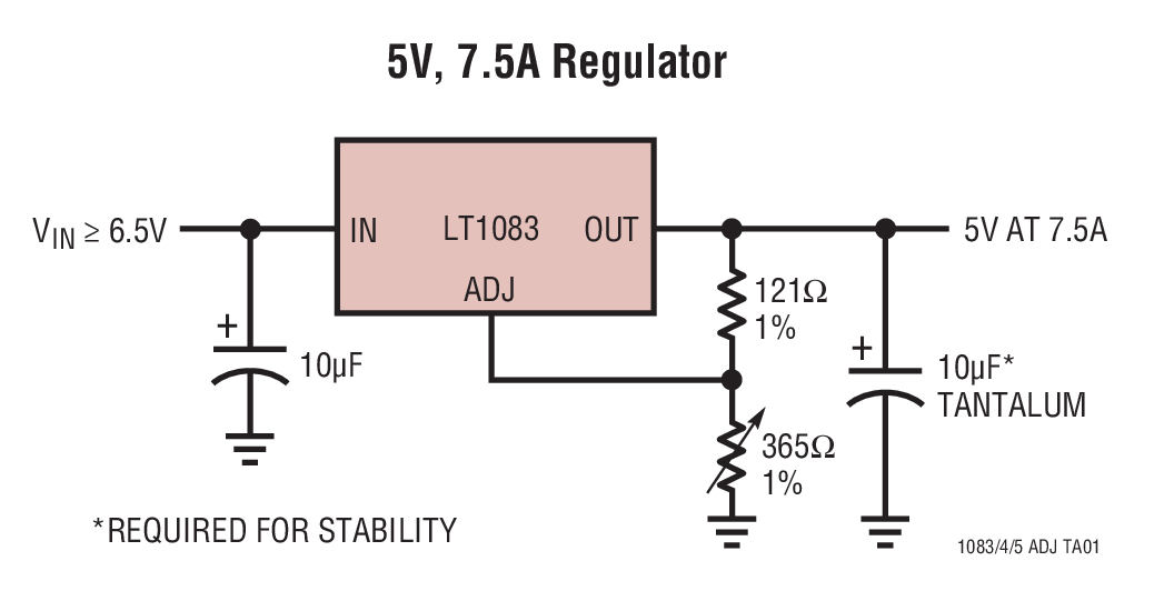
The figure below shows the typical application circuit for the LT1083 adjustable LDO. The external resistor values are calculated such that the circuit can deliver a constant 5V/7.5A output. The input and output capacitors are appropriately placed to eliminate the input voltage ripples, noise, and prevents device from instability.
Common Circuit Applications with LT1085 LDO
Due to it’s high output current capability, low dropout voltage, and excellent thermal performance, the LT1085 LDO is widely used in applications where clean, stable power is required.
Post-Regulation After Switching Power Supplies (SMPS)
One of the most practical and high-value uses of the LT1085 is as a post-regulator after a switching power supply. A switching power supply (SMPS) is used as the primary regulator because of its high efficiency and ability to handle large input-to-output voltage differences. However, SMPS outputs inherently contain switching ripple, high-frequency noise, and transient spikes, which can negatively affect sensitive electronic circuits. This is where LDO LT1085 comes into play!
Sensitive circuits such as microcontrollers, ADCs, DACs, RF modules, and audio stages require a clean, low-noise, and stable power rail to function reliably. The output of switch-mode power supplies contain high frequency switching noise and output ripple. Therefore, LT1085 is used as a post regulator after the SMPS so that the clean and noise-free output can be fed as an input to sensitive circuits like microcontrollers, ADCs, RF modules, and many more.
High-Current Linear Bench Power Supplies
Unlike switching regulators, linear power supplies do not generate high-frequency switching noise. This makes them ideal for applications where clean and stable voltage is required. In such situations, using a high-current linear power supply is often a good option.
A common high-current linear supply using the LT1085 typically includes an AC transformer that steps down the mains voltage, a bridge rectifier used to convert AC to DC, a bulk electrolytic capacitor that smooths the rectified DC, and an LT1085 LDO that provides precise voltage regulation.
This set up commonly used in testing and calibration equipment, industrial control panels, PLC subsystems, and actuator power rails.
Simulation Results: 5V / 3A Linear Power Supply Design Using the LT1085 adjustable LDO
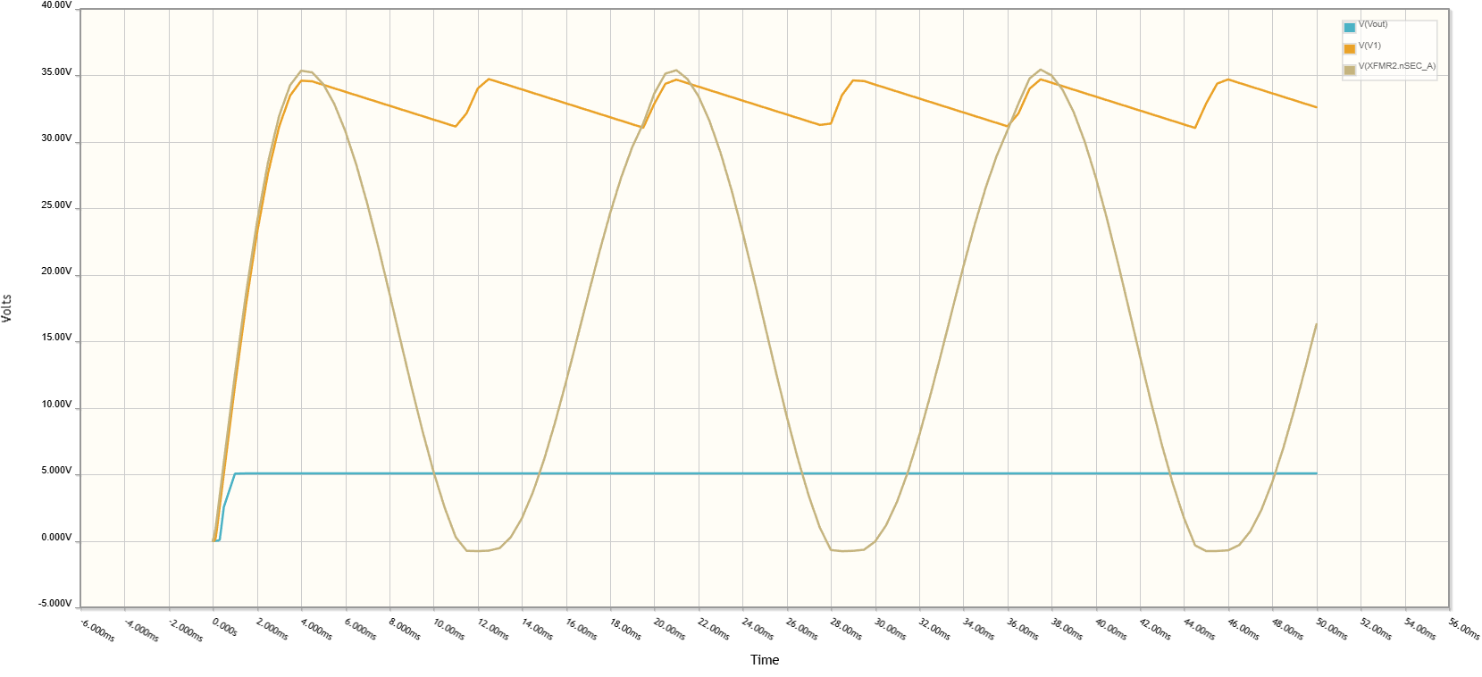
In this section, I have designed and simulated the 5V/3A power supply using the LT1085 LDO. The simulation demonstrates how AC mains power is converted into a stable, regulated 5V DC output capable of supplying high current.
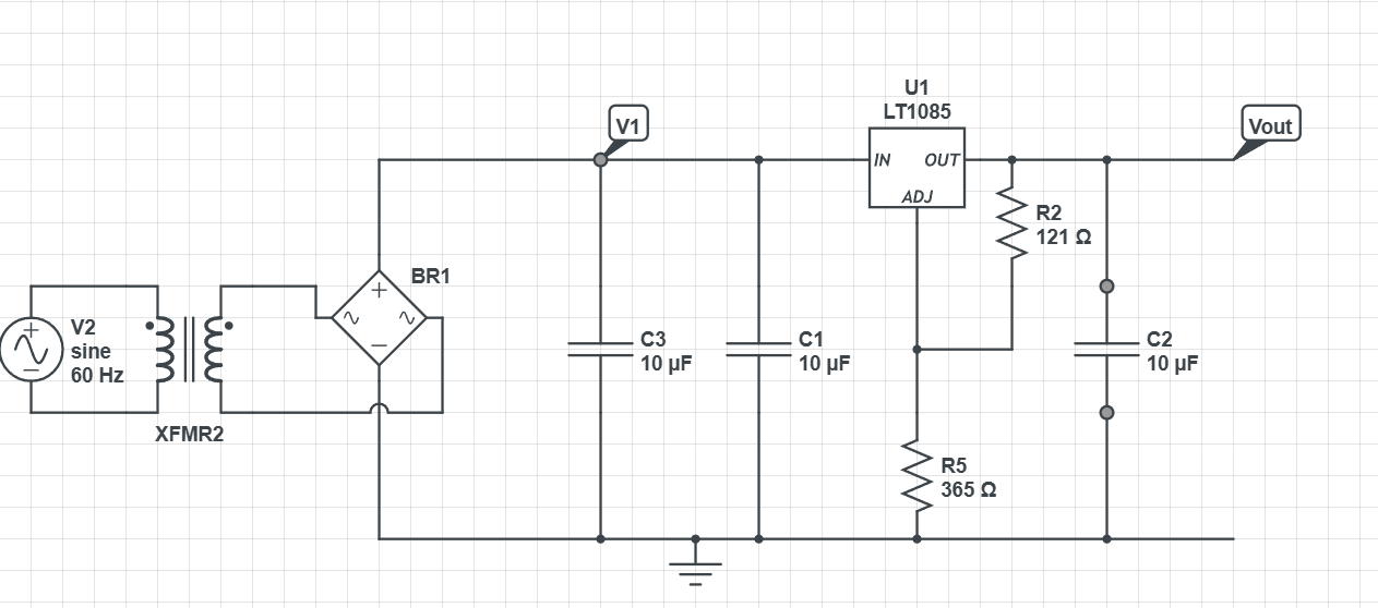
The 220VAC is taken from the main source, which is applied to a step-down transformer. The transformer reduces the high-voltage AC input to a safe low-voltage AC level suitable for rectification and regulation, as shown in the output waveform. The transformer output is fed into a full-bridge rectifier, which converts the low-voltage AC into pulsating DC. A bulk electrolytic capacitor is connected after the bridge rectifier to smooth the pulsating DC.
The filtered DC voltage is then applied to the LT1085 adjustable LDO, which performs the final voltage regulation as shown in the output waveform. It is worth noting that the input voltage remains above the dropout requirement, ensuring proper regulation. The output voltage is set using two external resistors: R1 = 121Ω, and R2 = 365Ω, using the formula in the datasheet. These resistors configure the LT1085 to produce a regulated 5V output, according to the datasheet equation.
LT1085 vs Alternatives
When selecting a high-current voltage regulator, the LT1085 is often compared with other linear regulators and modern switching solutions. Each option has strengths and trade-offs, and the right choice depends on current requirements, noise sensitivity, efficiency, thermal limits, and design complexity. The most common alternatives to LT1085 are LM338 and LM350. The comprehensive comparison between LT1085 and these LDOs is described below.
Comparison of LT1085, LM338, LM350, and Switching Regulators
Conclusion
To conclude, LT1085 LDO is one of the most versatile and reliable high-current linear regulators available for modern electronics. Its combination of low dropout voltage, high current capability (up to 3A), low noise, and robust thermal performance makes it ideal for applications where stable, clean power is critical. This technical tutorial includes LT1085 technical specifications, it’s circuit design, thermal design calculations, and practical circuit guide of 5V/3A power supply design.
Frequently Asked Questions (FAQ)
Input capacitor (Cin): ≥10µF electrolytic, placed close to the IN pin to filter voltage spikes
Output capacitor (Cout): ≥10µF electrolytic for stability; add 0.1µF ceramic in parallel for high-frequency noise suppression
Yes, by selecting the appropriate resistor values for the adjustable version or using a fixed 3.3V version, the LT1085 can reliably supply 3.3V at up to 3A, provided the input voltage is at least 4.5–5V to account for dropout.
Yes, but keep in mind that linear regulators waste power as heat. The LT1085 is most suitable for moderate voltage drops and high-current applications. For large voltage differences, a switching regulator or hybrid SMPS + LDO approach is recommended to conserve battery life.
The LT1085 can deliver up to 3A of continuous output current with proper thermal management. Exceeding this may trigger the internal current limit or cause thermal shutdown.
Yes. It is commonly used as a post-regulator after an SMPS to clean up ripple, reduce noise, and provide precise output voltage.