Introduction: Overcoming the Memory Wall
You learned about selecting the perfect component in Part 1. You explored the datasheet, and chose a Micron chip with the right density and temperature range. However, your work is not done yet. Even the best integrated circuit memory in the world will fail if you neglect the physical design.
The layout of your Printed Circuit Board (PCB) determines success. The link connecting the processor with the memory is the most important interface in your system. This interface operates at extreme speeds.
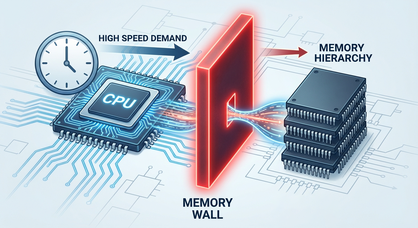
Engineers often come across a common challenge known as the Memory Wall. This is a bottleneck, and it occurs when your CPU processes data faster than it receives it from the memory chip. Hence, the processor sits idle, waiting for data to arrive from the memory chip. This destroys system performance.
You need to solve this through architecture and layout. High-speed interfaces like ddr4-2666 offer the raw speed to get out of the confines of this wall. Advanced micron memory architectures like LPDDR5 reduce latency. However, these speeds are only the theoretical limits, and the actual limit will depend on how good your physical layout is.
Signal integrity determines if a “1” remains a “1”, whereas the power integrity determines if the voltage stays stable. On the other hand, thermal management determines if the chip lasts longer. This guide shows you how to master these physical constraints.
Designing the Embedded Memory Hierarchy
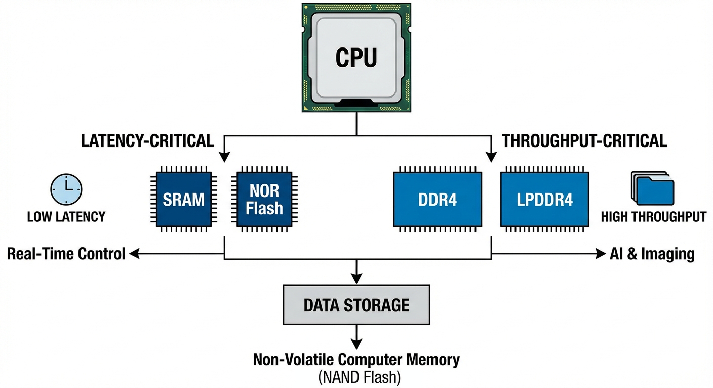
You must align your memory architecture with your data flow. Not all memory serves the same purpose, that is why you need to decide between latency-critical tasks and throughput-critical tasks.
Latency vs. Throughput: The Trade-off
Latency is the time your memory takes to start delivering data after the processor asks for it. Whereas, throughput is the amount of data you transfer over time. You rarely get highest of both in a single component.
Latency-Critical Applications
Real-time control loops require low latency. For example, an automotive braking system cannot wait longer, and a boot loader must execute immediately.
The Solution is that you use on-chip SRAM or fast XIP (Execute-in-Place) NOR Flash. This is because these technologies allow the CPU to access random addresses instantly. There is no setup time.
Throughput-Critical Applications
On the contrary, the edge AI and high-resolution imaging require high throughput. You move massive blocks of data, and do not care if the first byte takes a few nanoseconds longer. All you care about is the total volume transferred per second.
Here, the solution is to use high-bandwidth memory like DDR4 memory or LPDDR4. This is because these architectures use burst modes. They send data in quick chunks of packets once the channel opens.
DDR3L vs. DDR4: Choosing the Right Standard
You must choose the correct memory generation for your performance needs.
| Feature | DDR3L | DDR4 |
| Voltage | 1.35V | 1.2V |
| Max Speed | 1866 MT/s | 3200 MT/s |
| Prefetch | 8n | 8n (with bank groups) |
| Topology | T-Topology (Typical) | Fly-by Topology |
| Termination | On-PCB | On-Die (ODT) |
Bus Width and Organization
You control bandwidth by adjusting the bus width, where widening the bus from x8 to x16 or x32 increases throughput. It allows you to move more bits per clock cycle. Even though, this comes with a cost.
The Routing Penalty
A wider bus needs more traces on your PCB. An x32 interface would require a lot more space than an x8 interface.
You must match the length of 32 data lines instead of 8, increasing complexity.
You need more PCB layers to route these signals without crosstalk, requiring more space.
More lines mean more potential for noise coupling, a compromise on integrity.
Micron Part Integration
Micron offers the MT40A series to solve this. They provide various organizations to match your host controller. For example, you might choose an x16 part like the MT40A2G4SA-062E to save space on a small industrial controller, or you may choose two x8 parts for a system that needs ECC (Error Correction Code). However, you must verify your processor support before selecting the organization.
PCB Layout and Signal Integrity (SI)
Memory integrity depend on signal integrity. At high speeds, copper traces act like transmission lines. They are not simple wires, instead they have resistance, capacitance, and inductance. You must manage these properties.
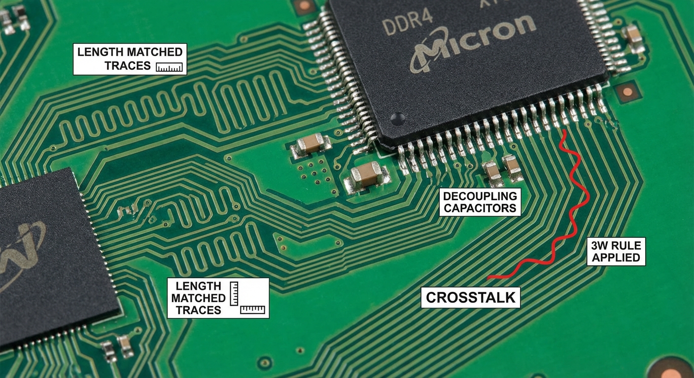
Length Matching: The Timing Budget
Electrons travel at a certain speed through copper, and this speed depends on the dielectric material of your PCB. In high-speed ddr4-2666 designs, data bits arrive in picoseconds.
If one trace is slightly longer than another, the data arrives late. We call this timing skew. If the skew is too large, the processor starts sampling the data at the wrong time. You read a zero instead of a one. The whole system crashes.
Actionable Rules for Matching:
- Group Signals: You must match data lines (DQ) to their strobe (DQS).
- Tight Tolerances: Keep length mismatches within +/- 0.5mm or better.
- Serpentine Routing: You sometimes see squiggly lines on memory PCBs. These add length to shorter traces to forces all signals to arrive simultaneously.
Termination and ODT
Likewise, the high-speed signals tend to bounce. When a signal hits the end of a trace, it reflects back to the source. This reflection collides with new incoming data, resulting in noise.
On-Die Termination (ODT)
Legacy memory required resistors on the PCB to stop reflections. However, modern micron memory chips use ODT. The termination resistor is inside the silicon die, helps save PCB space.
Better control is possible because the memory controller turns ODT on and off dynamically.
It absorbs the signal energy at the end of the line, preventing reflections and ensuring a clean data eye.
Fly-by vs. T-Topology
It is important that you choose the right routing topology for your address and command buses.
T-Topology
This was common for DDR2 and DDR3. You branch the trace like a letter T to reach two chips.
The advantage is that, in the ideal situation, the signals arrive at both chips at the exact same time. But the disadvantage is that it is difficult to route at higher speeds, because the stubs create signal degradation.
Fly-by Topology
This is the standard for DDR4 memory, where you route the signal to the first chip, then the second, then the third in a chain.
It eliminates stubs, and improves signal quality quite a bit. However, the signals arrive at chips at different times. But you can fix this by using write leveling in your initialization software. The controller learns the delay for each chip and adjusts accordingly. For more technical details on DDR4 routing specifications, please refer to the JEDEC standards.
Impedance Control
Moreover, you cannot ignore impedance. DDR4 memory requires specific impedance values to function properly. The impedance for the single-ended traces is 50 Ohms, while for differential pairs (Clock/Strobe), it is 100 Ohms.
You can achieve this by controlling trace width and the distance to the reference plane. This requires working closely with your PCB fabrication house. They will tell you the exact stack-up to use. If you miss the target impedance, you get signal reflections. No software will be able to fix this.
Crosstalk Prevention
Signals travelling on parallel trace interfere with each other. This is crosstalk. A switching signal induces a voltage on its neighboring trace. To prevent this, you should:
- Follow the 3W rule by keeping the center-to-center distance between traces at least three times the trace width.
- Implement separation by grouping your byte lanes. Keeping a large gap between Data Group 0 and Data Group 1.
- Respect the reference planes, and never route high-speed memory signals over a split in the ground plane. The return current needs a solid path. Crossing a gap creates massive EMI (Electromagnetic Interference).
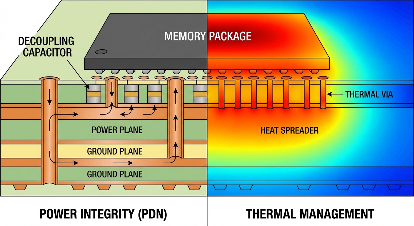
Power Integrity (PDN) and Thermal Management
Your memory chip is actually a dynamic load because it draws current in sharp spikes. When it executes a refresh command, current consumption jumps instantly. Your Power Distribution Network (PDN) must be capable of handling this.
The Role of the PDN
The PDN delivers stable voltage to the silicon die. If the voltage drops during a current spike, the logic gates slow down, and data corruption occurs. This is a main cause of integrity memory failure.
Target Impedance
You should treat the PDN as an impedance challenge, where the goal is to Keep the impedance of the power rail low across all frequencies.
It is expressed by the formula:
\[Target Impedance=\frac{Allowed Voltage Ripple}{Maximum Transient Current}=\frac{60×10^{-3}V}{2A}=0.03Ω\]
This means that if you allow 60mV ripple and the chip pulls 2A, your PDN impedance must be below 0.03 Ohms.
Capacitor Selection and Placement
You can also use decoupling capacitors to lower the impedance. A single capacitor is not sufficient. Therefore, you need a mix.
Bulk Capacitors
These store large amounts of energy, and easily handle low-frequency demands. You need to place them near the memory voltage regulator.
Ceramic Capacitors (MLCC)
These respond fast. They handle high-frequency noise, and you must place these as close to the memory pins as possible
Keep in mind that you should use Capacitors with low ESL (Equivalent Series Inductance). Also, the reverse geometry capacitors (long and wide) offer lower inductance.
For mounting, you must use vias immediately at the capacitor pads. Long traces add inductance. Inductance blocks the flow of high-frequency current.
Thermal Constraints in Embedded Systems
High-density micron memory generates heat. LPDDR and NAND chips get hot during write operations. In a fanless industrial enclosures, this heat has nowhere to go.
Heat Generation
Mainly it is due to the active power which is consumed during reads and writes. Also, background power that is consumed during standby contributes in heating too.
Another cause of heating is leakage, where a silicon gets hotter, it leaks more current. This creates more heat. This is called thermal runaway.
Thermal Design Calculation
You must verify the thermal design mathematically using the junction temperature formula:
\[T_J=T_A+(P_D×θ_{JA})\]
- TJ : Junction Temperature (Max limit from datasheet).
- TA : Ambient Temperature inside the box.
- PD : Power Dissipation (Watts).
- θJA : Thermal Resistance (Junction-to-Ambient).
Example Calculation:
Your system runs at 85°C ambient. The memory consumes 0.5W. The θJA is 20°C/W.
\[T_J=85+(0.5×20)=95°C\]
If the datasheet max is 95°C, you are at the limit. You need to use thermal vias under the BGA pad or copper pours to decrease.
Mitigation Strategies
You must design the PCB such that it removes the heat using various methods, such as:
Thermal Vias: Place vias under the central ground pad of the BGA. These transfers heat from the die to the internal copper planes.
Copper Pours: Using large copper areas on outer layers acts as a heat spreader.
Junction Temperature: Respect the max (Case Temperature) in the Micron datasheet. If you exceed it, data retention will likely fail.
Functional Safety and Error Correction
Memory integrity is non-negotiable, especially in industrial and automotive sectors. Think in this way, a bit flip in a video game only causes a glitch, whereas a bit flip in a steering system will cause an accident.
Automotive Functional Safety (ISO 26262)
You must adhere to strict standards for automotive designs. For this reason, ISO 26262 standard defines the ASIL (Automotive Safety Integrity Level).
For the proper risk Assessment, you must evaluate the risk of memory failure. To reduce the risk, redundancy is important, where critical systems come with redundant memory paths.
Therefore, Micron memory products, such as Micron LPDDR4 MT53E256M32D2DS, always possess ASIL certifications. Their design aims for zero-defect approach.
ECC (Error Correction Code)
ECC detects and fixes errors. There are two main types you should understand.
Internal ECC
This is common in non-volatile memory like NAND Flash and some LPDDR components.
Function wise, the logic inside the memory chip handles error correction.
In practical cases, its duty is to correct single-bit errors caused by cell degradation or background radiation.
The correction is transparent, where the host processor does not know an error occurred. It receives clean data.
Host ECC
ECC at host is a system-level approach. The processor generates a checksum for every data word.
However, this requires additional hardware, where you need an extra memory chip (x72 width instead of x64) or a specialized controller.
Function wise, when a bit flip occurs during transmission or storage, the processor detects it.
Correction wise, host ECC corrects single-bit errors and detects multi-bit errors. This protects the CPU workspace from corruption.
The Future of Memory and Storage
Looking ahead, the future of memory and storage is all about safety. As vehicles become autonomous, the demand for error-free memory increases. The market will see more on-die safety features in standard DRAM components. Therefore, you must prepare your designs for this shift now by selecting ASIL-ready components.
Validation and Sourcing Reliability
When you finish the layout, and get the board fabricated. It’s about time you prove it works.
Stress Testing and Margins
Simply turning on the power on is not the reliable indicator of working correctly. Instead, you need to stress the system. You can do this by Temperature cycling, Voltage Margining, and Clock Margining.
Temperature cycling involve running the memory at -40°C and +85°C (or +125°C).
Moreover, voltage margining is when you lower the voltage by 5%. Raise it by 5%, and then see if the memory still passes.
Finally, clock margining involves pushing the frequency slightly higher. If it fails immediately, this indicates that your signal integrity margin is too low.
These tests can expose weak solder joints and poor impedance control. They help you make sure your integrity memory design works and lasts in the field.
The Role of the Distributor
No matter how good your design is, it is bound to fail if the physical component is not good. The electronic component market is flooded with counterfeit parts. A fake memory chip will fail your stress tests. It will surely fail in the field.
Traceability is Key
The solution is to source your parts from authorized distributors. Sourcing through Flywing guarantees authenticity. You get full traceability back to the Micron factory. At Flywing, lifecycle management is key.
Industrial products are designed for 10 years. You need a partner who manages End-of-Life (EOL) notifications. You cannot afford to redesign your board every two years because a grey-market vendor ran out of stock.
Legitimate sourcing ensures you meet trade compliance and environmental standards. Therefore, Flywing ensures Compliance with RoHS/REACH.
Conclusion
A high-quality micron memory chip is utilized best with a high-quality PCB layout. A compromise on one with render other useless. Importantly, the physical design defines the performance limit. You faced the Memory Wall. This article helps you learn how to break it with hierarchy and layout.
Moreover, you now understand that DDR3L and DDR4 memory are not just logic blocks, instead, they are complex analog systems. You need to manage signal reflections with termination, and manage power delivery with low-impedance networks. Furthermore, you know how to control heat with thermal vias.
If you ignore one or more of these rules, you are prone to random crashes. You get data corruption. You get field returns.
Likewise, if you follow these rules, you create a system that is robust, reliable, and survives longer in harsh industrial environments.
You know that memory integrity is invisible to the end-user. They never see the trace matching, or the decoupling capacitors. What they see is the system that works. Therefore, it is your responsibility to make sure the optimal outcome through rigorous design and sourcing quality parts.
For a reliable, traceable supply of high-integrity Micron memory solutions, visit the Flywing Memory Category to check inventory and request quotes.
Frequently Asked Questions
A Power Distribution Network, in short PDN is an interconnected system of traces, planes, and capacitors that powers the memory chip. It is important because memory chips draw current in large spikes. A weak PDN causes voltage drops, leading to data being corrupted as well as system instability.
In this case, you should use a fly-by topology for address and command signals, and match trace lengths within strict tolerances (picoseconds). Also, you must maintain continuous ground reference planes and use the correct termination (ODT) settings.
Non-ECC memory stores data, but it is not able to verify it. On the other hand, ECC memory includes extra bits to identify and fix data corruption. ECC is quite important for safety-critical systems in automotive and industrial sectors to prevent crashes brought on by random bit flips.
The Memory Wall is a bottleneck, it happens when the CPU work faster than the memory. The CPU sits idle waiting for data from the memory. This is performance limiting, especially in data-intensive applications like Edge AI. You overcome this with faster memory interfaces (like DDR4) accompanied by optimized layout.
Yes. High-speed non-volatile memory like NAND Flash or eMMC work with fast interfaces. Therefore, poor signal integrity on these lines causes read/write errors, lead to operating system corruption, and reduces the actual speed of the storage.
Edge AI needs large dataset processing that too in real-time. DDR4-2666 provides higher bandwidth (and throughput) than slower counterparts. This is to make sure the AI processor receives image or sensor data fast enough to make decisions without lag.