The EPC23101 is a 100 V monolithic GaN IC from Efficient Power Conversion (EPC) that integrates a high-side eGaN FET (3.3 mΩ RDS(on) max / 2.6 mΩ typical), a half-bridge gate driver, input logic interface, level shifting, and synchronous bootstrap charging — all in a single thermally enhanced QFN. Paired with the EPC2302 external low-side FET (1.4–1.8 mΩ), it forms a 65 A ePower Chipset capable of over 1 MHz switching and up to 97% efficiency in a 48 V-to-12 V buck converter within a combined 7 × 5 mm footprint.
Important: the official errata limits safe operating VIN to 60 V maximum, not 100 V.
| Parameter | Value |
|---|---|
| HS FET RDS(on) max | 3.3 mΩ |
| Peak efficiency @ 500 kHz | 97% |
| Max output current | 65 A |
| Max switching frequency | > 1 MHz |
What Is the EPC23101?
The EPC23101 is a 100 V-rated monolithic gallium nitride (GaN) IC introduced by Efficient Power Conversion (EPC) in December 2021. It is part of EPC’s ePower™ Stage IC family– a lineup designed to simplify power converter design by integrating the most parasitic-sensitive components into a single chip, including the high-side FET and its associated gate driver circuitry.
The EPC23101 differs from earlier EPC high frequency devices, such as EPC2152 (which is a fully integrated dual-FET half-bridge with both transistor drivers and sharing the same die. In contrast, the EPC23101integrates only the high-side FET on chip and provides a gate driver output (LGOUT) to drive an external low-side FET. This approach gives designers greater flexibility, as they can independently select and size each FET based on current requirements, asymmetrical duty cycle loss distributions and thermal management considerations _something that is not possible with fully symmetric monolithic designs.
Technology Platform — GaN-on-Silicon
The EPC23101 is manufactured using EPC’s exclusive GaN on Silicon (GaN on Si) process utilizing Enhancement Mode GaN (e-mode) transistors. As with many of today’s conventional MOSFET transistors, e-mode GaN transistors are normally off until a sufficiently high positive voltage is applied to the gate, allowing them to turn on; thus eliminating the need for a negative gate supply and greatly simplifying the design of the gate drive circuit.
Compared to silicon, GaN has a distinct material advantage as it possesses no reverse recovery charge (Qrr = 0). In other words, silicon MOSFETs retain some minority carrier charge in the body diode while turned-on and the reverse recovery charge must be cleared out during turn-off, resulting in a current spike, energy lost during switching, and placing a hard cap on the maximum allowed frequency of switching. In the case of GaN, there is no body diode to negate reverse current conduction; rather, GaN devices are based on drain-source conduction when the gate-source voltage is 0, thus not generating any recovery charge. This key specification provides GaN converters with the ability to switch at MHz frequencies and operate at overall efficiencies that are not possible with silicon devices.
The lateral architecture of GaN-on-Si enables EPC’s process engineers to integrate multiple logic- level devices on the same die as the power transistor, including an input buffer, level shifter, bootstrap charge switch, and under-voltage lockout comparator. The co-integration forms the physical foundation of the monolithic architecture used in the EPC23101.
Product Summary
| Parameter | Value / Description |
|---|---|
| Manufacturer | Efficient Power Conversion (EPC) |
| Device Type | eGaN IC — Integrated HS FET + Gate Driver |
| Structural VDS | 100 V |
| Max Operating VIN | 60 V (Errata v1.2) |
| RDS(on) Typical | 2.6 mΩ |
| Gate Charge Typical | 3.5 nC |
| ⚠ Note: Values are typical. Max VIN is limited per Errata v1.2. Ensure PCB layout follows EPC recommended guidelines for gate drive and HS FET connections. | |
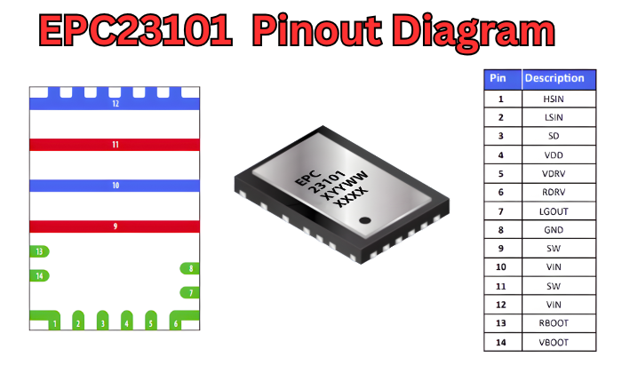
EPC23101 Pinout Diagram & Pin Descriptions
Package Description — QFN with Exposed Top Pad
The EPC23101 comes in a thermally enhanced QFN package featuring an exposed top thermal pad. Unlike conventional QFN packages that use an exposed bottom pad, this design enables direct attachment of a heat sink or heat spreader to the top surface of the die, where heat is most effectively dissipated. With proper thermal interface material (TIM) selection and forced convection, the junction-to-ambient thermal resistance can be significantly reduced, resulting in improved thermal performance and higher current capability under elevated ambient conditions.
All exposed pads have flanks that allow for wetting confirmation by automated optical inspection (AOI) systems for side inspection of the solder joint quality from the side of the package. This is a production quality-control benefit that is advantageous for high-volume manufacturing. The minimum spacing distance between HV and LV pads is no less than 0.6 mm on the package and complies with IPC creepage and clearance requirements for the device’s voltage class.

Complete Pin Function Reference
The table below provides a complete functional description of every pin. Pin type codes follow EPC’s convention: P = Power, S = Bias Supply, L = Logic Input/Output, G = Gate Drive Adjust.
Power Pins:
| Pin Name | Type | Function Description |
|---|---|---|
| VIN | ⚡ P — Power | Power DC input. Connected to the drain terminal of the internal high-side GaN FET. Decouple with power loop capacitors from VIN to PGND placed as close to the device pads as physically possible. |
| SW | ⚡ P — Power | Switching node. Source of the internal HS FET and drain of the external LS FET. ⚠ Highest dV/dt node Keep all sensitive signal traces away from SW copper. |
| PGND | ⏚ P — Power | Power ground. Connected to the source terminal of the low-side FET. Return point for all high-current switched paths. |
| AGND | ⏚ P — Power | Analog ground. Internally shorted to PGND. Used as the reference for all logic and analog circuits. Connect to PGND at single star point |
Supply Pins
| Pin Name | Type | Function Description |
|---|---|---|
| VCC | ⚡ S — Supply | Internal logic supply voltage. Provides power to the internal gate drive and analog circuits. Decouple with 1µF–4.7µF ceramic capacitor close to the pin. |
| VCC_LS | ⚡ S — Supply | Low-side FET supply. Supplies the gate driver of the internal low-side FET. Typically connected to a bootstrap capacitor between SW and VCC_LS. Bootstrap required |
| VCC_HS | ⚡ S — Supply | High-side FET supply. Supplies the gate driver of the internal high-side FET. Typically powered through a bootstrap network (SW to VCC_HS capacitor) for proper high-side operation. |
Logic Pins:
| Pin Name | Type | Function Description |
|---|---|---|
| EN | 🔹 I — Input | Enable pin. When high, the device is active and switching. When low, the device enters a low-power shutdown mode. |
| PWM | 🔹 I — Input | PWM control input. Drives the duty cycle of the internal GaN FETs. Compatible with 3.3V or 5V logic levels. |
| FAULT | 🔹 O — Output | Fault indicator output. Open-drain output that goes low during overcurrent, overtemperature, or UVLO events. Connect to a pull-up resistor to VCC. |
| OTW | 🔹 O — Output | Overtemperature warning output. Open-drain signal that goes low when die temperature approaches thermal limit. Use to signal thermal throttling or initiate cooling. |
Gate Drive Pins:
| Pin Name | Type | Function Description |
|---|---|---|
| GH | 🔹 O — Output | Gate drive output for the high-side GaN FET. Provides fast, high-current switching pulses to the GH pin of the internal FET. Keep traces short and low-inductance. |
| GL | 🔹 O — Output | Gate drive output for the low-side GaN FET. Delivers precise switching pulses with minimal delay and overshoot. Short, low-inductance PCB paths are essential. |
| VS | 🔹 I — Input | High-side FET return node. Connected to the source of the high-side FET. Used as the reference for GH switching and bootstrap operation. Keep connection tight to minimize loop inductance. |
| LO | 🔹 O — Output | Gate drive output for low-side FET. Directly drives the LO pin of the low-side FET. Must be routed with minimal parasitic inductance to maintain fast switching. |
Functional Architecture & Internal Block Diagram
Five functional subsystems (i.e., (1) high-side eGaN power FET, (2) input logic with PWM filtering, (3) high-side/low-side level shift logic, (4) synchronous bootstrap charging logic, and (5) gate drive buffer circuits for both internal HS FETs and external LS FETs) are integrated in the EPC23101 Gan FET as an integrated GaN-on-Si die. Understanding how these subsystems interact is essential for achieving a proper design, which includes startup sequencing, dead-time configuration, gate drive tuning, and errata hazard mitigation.

Synchronous Bootstrap Charging Circuit
In Conventional gate driver ICs, the floating high-side bootstrap supply is typically charged using a small Schottky diode that forward-biases during low-side conduction intervals. The EPC23101 replaces this diode with a synchronous GaN FET in the bootstrap charging path. The difference is material to both efficiency and design simplicity.
The synchronous bootstrap GaN FET produces a dropout voltage of approximately 100 mV, compared to approximately 600 mV for a conventional Si Schottky bootstrap diode.
Because VBOOT is maintained closer to VDD, the high-side gate drive circuit achieves consistent gate current and stable switching delay across the full duty-cycle range — delivering a clear efficiency and timing advantage.
Additionally, the GaN bootstrap FET has zero reverse recovery charge, eliminating energy loss that occurs in diode-based bootstrap designs during reverse-bias transitions.
The correct sequencing of the start-up process is critical to the proper function of the IC. At start-up, the bootstrap capacitor CBOOT starts at zero volts. After HSIN and LSIN start switching, the IC includes a nominal six-cycle delay before the high-side gate drive output will closely track your PWM inputs. This allows the bootstrap to build enough charge for reliable turning on of the HS FET, and this is done entirely inside the IC — no need for external startup sequencing logic.
The bootstrap FET will only be activated after the low-side FET (Q2) has been turned on during the current switching cycle, thus there will be no risk of overcharging CBOOT during a dead-time period. If VDRV is present but VIN is < minimum operating voltage, then the pass transistor from VDRV to VDD is disabled, and all remaining charge on the VDD bypass capacitor will be discharged through the internal circuits of the IC.
Level Shifting and Noise Immunity
The level shifter transfers PWM signals from the low side, referenced to AGND, to the high side, which floats up to VIN (60V operational, according to errata). EPC’s level shifters are designed to remain stable under significant negative transients at the SW node, a common occurrence in hard-switching regulators where the SW rail can ring below ground during the turn-on transitions.
Both HSIN and LSIN are fitted with an input pulse filter, which blocks any pulses shorter than about 15 ns. These onboard filters prevent noise spikes, PWM glitches, and transients from reaching the power MOSFETs’ gates. As noted in Errata point 3, pulses shorter than the minimum pulse width (PW_MIN), which is less than the 15 ns filter, may cause latch-up events. Designers should ensure that the PWM controller’s minimum on- and off-time exceeds PW_MIN in all operating conditions.
Under-Voltage Lockout (UVLO) and Cross-Conduction Prevention
Both high-side and low-side under-voltage lockout (UVLO) circuits monitor the gate drive supply voltage for each FET. If either supply falls below the UVLO threshold, the corresponding FET is immediately turned off. In addition, if both voltages fall below UVLO levels but the input voltage (VIN) is still above 10V, a separate protection circuit activates to prevent any shoot-through during the supply collapse transient. An additional circuit that actively pulls down the gate of each FET is connected to VIN, and it will also prevent the destructive turn-on of FETs due to gate-to-drain leakage current when the FET is in its off-state.
The cross-conduction prevention logic simultaneously monitors HSIN and LSIN. If HSIN and LSIN both assert the high (active) level at the same time, the IC keeps both FETs off until one condition clears and then waits a predetermined t_lockout before enabling the appropriate FET. This hardware lockout provides an additional layer of protection but does not replace the need for correctly programmed dead time in the external PWM controller.
Gate Drive Timing and Tuning
Both the rise and fall times of the EPC23101 Gan FET can be adjusted between 1 and 3ns (0 to 48 V swing at maximum load) using external resistor on the RBOOT (for the high-side) and RDRV (for the low-side). Faster switch transitions reduce switching losses, while slower transitions help limit peak time over-voltage at SW node. Since the SW over-voltage spikes can exceed 70 V — the absolute maximum SW transient rating — Errata Sheet v1.2 specifies that both resistor values must be at least 3.3Ω. Designers who previously used lower resistor values may therefore experience SW over-voltage spikes above 70 V.
Electrical Characteristics & Key Specifications
DC Characteristics — HS FET and System
| Parameter | Condition | Typical | Max | Unit |
|---|---|---|---|---|
| HS FET RDS(on) | VGS = 5 V, TJ = 25°C | 2.6 | 3.3 | mΩ |
| LS FET RDS(on) (EPC2302) | VGS = 5 V, TJ = 25°C | 1.4 | 1.8 | mΩ |
| VIN Operating Range | All conditions | 48 (nominal) | 60 (Errata) | V |
| VDRV Supply Range | — | 5.0 | 5.5 | V |
| HS FET Reverse Conduction Voltage | Normal operation | 2 | — | V |
| HS FET Reverse Conduction (Boost Mode) | Non-switching, Errata ERR-4 | >4 (typical) | — | V |
Switching and Logic Characteristics
| Parameter | Condition | Typical | Unit |
|---|---|---|---|
| Max Switching Frequency | Full load, VIN = 48 V | >1,000 | kHz |
| Gate Drive Rise / Fall Time | RBOOT / RDRV tuned | 1 – 3 | ns |
| Logic Input Threshold (H) | HSIN, LSIN (3.3 V / 5 V CMOS) | — | V |
| Input Pulse Filter Rejection Width | Pulses below this value rejected | 15 (typ) | ns |
| SW Over-Voltage Limit | With RBOOT / RDRV ≥ 3.3 Ω (Hard switching) | ±10 (from rail/GND) | V |
| SW Node Absolute Max Transient | Absolute maximum (Errata) | — | 70 V (MAX) |
| Startup Delay (CBOOT Charge) | After HSIN / LSIN begin switching | 6 switching cycles | — |
| RBOOT, RDRV Minimum Value | Per Errata v1.2 | 3.3 Ω minimum | Ω |
Thermal Characteristics
The exposed top pad is the main thermal path. When attached to a top-side heatsink and receiving 500 LFM of forced airflow, the EPC23101 + EPC2302 chipset will provide 65 A of current in a 48 V-to-12 V buck converter with a temperature rise of less than 50°C above a 25°C ambient temperature. All output current and PWM frequency ratings in the datasheet are specified at TA = 25°C; however, thermal derating curves should be examined to evaluate the operation of the EPC23101 + EPC2302 chipset at higher ambient temperatures.
The type of thermal interface material used (TIM) has a large impact on junction-to-heatsink thermal resistance. While TIMs with electrical conductivity offer a lower resistance compared to insulating TIMs, they require that the heatsink be isolated if the exposed pad is not grounded. The datasheet provides both typical parameters for conducting and insulating TIMs in order to assist in thermal budgeting by the designer.
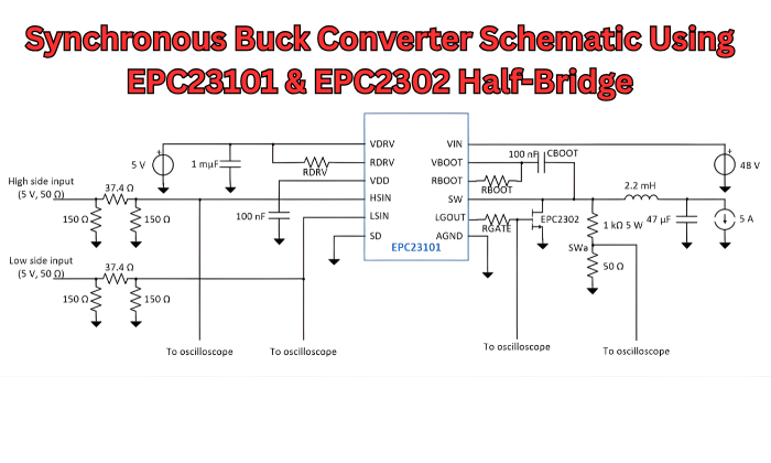
EPC23101 + EPC2302 — ePower Chipset Configuration
EPC developed the EPC23101 and EPC2302 to work together as part of their ePower Chipset, and they have complementary, optimized pinout layouts. Both chips’ SW pins (the HS FET source) and drain pins (the LS FET drain) are located in the same position on the PCB. This allows for a very tight critical power loop distance between HS source and LS drain connections without requiring any special routing methods. To make it easier for designers to move from traditional discrete MOSFET + Driver solutions to EPC’s ePower chipsets, EPC has created this pin-compatible solution.
| Parameter | EPC23101 (HS IC) | EPC2302 (LS FET) |
|---|---|---|
| Device Type | Integrated GaN IC (HS FET + full driver) | Standalone eGaN FET |
| Max Voltage | 100 V structural | 100 V structural |
| RDS(on) Typical | 2.6 mΩ | 1.4 mΩ |
| RDS(on) Maximum | 3.3 mΩ | 1.8 mΩ |
| Gate Charge (QG) | Internal — driven by IC | Very small — key switching advantage |
| QGD, QOSS | Integrated into IC drive design | Minimised for low switching loss |
| Package | Thermally enhanced QFN (exposed top) | Thermally enhanced QFN (exposed top) |
| Unit Price (1kU) | $5.28 | $4.91 |
| Combined Footprint | 7 mm × 5 mm (both devices) | 7 mm × 5 mm (both devices) |
Verified Efficiency Performance
EPC has published measured efficiency data for the EPC23101 + EPC2302 chipset operating in a 48 V-to-12 V synchronous buck converter, evaluated on the EPC90142 development board under defined thermal conditions.
| Switching Frequency | Peak Efficiency | Max IOUT | Temperature Rise | Reference / Application |
|---|---|---|---|---|
| 500 kHz | 97% | 65 A | <50°C | EPC90142, 48 V DC-DC |
| 1 MHz | 96% | 65 A | <50°C | EPC90142, high-density |
| 500 kHz (bidirectional) | >96.5% | 60–110 A | — | EPC9170 (2 kW converter) |
| 500 kHz (bidirectional) | 95.8% | 140 A | — | EPC9170 full load |
Test conditions: VIN = 48 V, VOUT = 12 V, DCR = 700 µΩ, L = 2.2 µH, TA = 25°C, 500 LFM airflow, top-side heatsink attached. Source: EPC application documentation.
EPC90142 Development Board
The EPC90142 is EPC’s dedicated evaluation platform for both the EPC23101 and EPC2302 chipsets. It is a half-bridge evaluation board with a maximum voltage of 100V and maximum current of 65A, measuring 2.0” x 2.0” (50.8mm x 50.8mm) and contains all of the critical components required to immediately evaluate the switching performance, along with a set of Gerber files and a Bill of Materials (BOM) to expedite custom PCB development. This evaluation board is priced at $156.25 and is highly recommended as the first step in hardware verification prior to committing to custom PCB layout.
EPC23101 vs. EPC2152 — Architecture Selection Guide
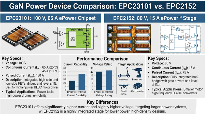
Engineers approaching EPC’s product family for the first time often consider the EPC2152 — a fully monolithic dual-FET half-bridge IC — alongside the EPC23101 chipset. The two architectures represent fundamentally different design trade-offs, and the right choice depends primarily on output current requirements, available PCB area, and whether asymmetric RDS(on) optimisation between the high-side and low-side transistors is needed.
| Criteria | EPC23101 + EPC2302 (Chipset) | EPC2152 (Monolithic) |
|---|---|---|
| HS FET RDS(on) Typical | 2.6 mΩ | 8.5 mΩ (symmetric) |
| LS FET RDS(on) Typical | 1.4 mΩ | 8.5 mΩ (symmetric) |
| Max Output Current | 65 A | Lower — suitable for <20 A |
| Package Footprint | 7 mm × 5 mm (two devices) | 3.85 × 2.59 mm (one device) |
| FET Design Flexibility | Independent HS/LS selection | Fixed symmetric FETs |
| BOM Complexity | 2 ICs | 1 IC |
| Design Engineering Effort | Moderate | Lower |
| Best Application Fit | >20 A, 48 V bus, high power density | <20 A, ultra-compact, cost-sensitive |
Select the EPC23101 chipset when output current requirements exceed approximately 20 A, when asymmetric RDS(on) optimization is beneficial (the LS FET conducts longer in high duty-cycle buck converters), when operating a three-phase motor drive that requires a balanced floating half-bridge, or when the application benefits from the independently measurable and replaceable high-side and low-side components.
The EPC2152 remains the better choice for highly space-constrained designs below 20 A, where BOM simplicity and board area outweigh conduction loss reduction.
Application Circuits & Reference Designs
EPC has launched various reference designs showing the EPC23101 in all of its main application fields. Each reference design provides characterised data regarding the efficiency data, Gerber files, and a Bill of Materials (BOM). The four principal areas of application are outlined below.
Application 1 — 48 V DC-DC Buck Converter (Data Centre / AI Infrastructure)
The EPC23101 and EPC23002 Chipset are primarily used for high-density datacenter point of load (POL) power conversion, as well as some high-density computing shelves, datacom equipment, and AI accelerator boards. The 97% efficiency at 500 kHz of this chipset will save significantly on cooling costs and increase the power density of racks that utilize these chips versus comparable silicon-based (Si) MOSFET solutions.
Operating at 500 kHz-1 MHz instead of 300-400 kHz, typical to silicon MOSFET designs, allows for about a proportional decrease in output inductor and filter capacitance versus the increase in frequency, which results in a measurably smaller magnetic footprint. The combination of the EPC23101/EPC23002’s output capability (65A), size (7mm x 5mm), and < 50 °C temperature rise at rated current makes them ideally suited to the new architectures provided by 48V busses being implemented in hyperscale datacenters today.
Application 2 — Three-Phase BLDC Motor Drive (E-Mobility, Robotics, Drones)
The EPC9173 reference design presents the EPC23101 utilized as a tri-phase inverter in the 48 V brushless DC (BLDC) motor driving applications for e-bikes, e-scooters, robotic arms, industrial drones, and power tools. Each phase leg uses two EPC23101 ICs with cross-connected PWM signals — a configuration that is less obvious than a simple driver + two FET arrangement, and that delivers a specific performance advantage worth understanding in detail.
In the standard configuration, the EPC23101 drives its internal High-Side FET from HSIN, while the EPC2302 drives its High-Side FET and gate driver from LSIN. When used in the EPC9173 cross-connected motor drive, this interconnection changes: the PWM signal for the opposite switch is fed into the Low-Side Input of one EPC23101. The first EPC23101’s external LG_OUT then drives the internal High-Side FET of the second EPC23101. This configuration forms balanced half-bridges where both switches float relative to power ground, enabling simple source shunt current measurement without any ground bounce at the PWM input nodes.
The EPC9173 board also incorporates a configurable over-current protection circuit that can function as either a hard over-current shutdown or a current-limiting function, depending on the motor controller algorithm and modulation strategy.
Application 3 — Bidirectional 48 V/14 V Converter (EPC9170)
The EPC9170 is a bidirectional DC-DC converter that can run on two separate phases. One is a 48V power bus, while the other is a 12V-14V power source for vehicles and industrial systems. It provides 2 kW of continuous power at a switching frequency of 500 kHz. Using GaN FETs results in low power loss during operation with efficiencies above 96.5% for output currents between 60A and 110A (as measured at the output terminals). For a maximum current of 140A, the converter operates at 95.8% efficiency. The EPC23101 includes integration of the gate driver within the IC, providing lower parasitic losses compared to using a discrete driver + FET combination, which ultimately leads to improved converter efficiency figures.
Application 4 — Solar MPPT and Industrial Power Converters
Maximum power point tracking (MPPT) converters for photovoltaic (PV) systems have very high switching frequencies due to their need to dynamically track the current/voltage (I-V) curve of a solar array and operate at high efficiency over a wide range of input power levels. The EPC23101 chipset can handle 48V solar string inputs and has adequate structural voltage (100V) for transient protection while load switching and during disturbances on the grid to ensure continuous operation. Additionally, this device has low switching losses to enable high efficiency during partial load conditions when the converter will typically operate at less than rated power for the majority of its operational hours.
PCB Layout Guidelines
Compared to typical Si MOSFET designs—where layout-related parasitic inductance has minimal impact—the layout of GaN (gallium nitride) FETs becomes much more critical. At switching frequencies of 500 kHz to 1 MHz, poor layout can lead to significant ringing, reduced efficiency, increased electromagnetic interference (EMI), and even potential device damage. The guidelines below are based on the EPC90142 reference board layout and EPC application notes.
Power Loop Layout — Highest Priority
The power loop can be defined as the parasitic inductance that is created by the path from the VIN decoupling capacitor(s) to the VIN pin of EPC23101, through the SW node, to the EPC2302 source, to PGND, and then back to the decoupling capacitor. Even a few nanohenries of inductance in this loop can significantly increase switching transients and output ringing.
- VIN-to-PGND decoupling ceramic capacitors should be placed right next to the VIN and PGND pads of both devices. Even a trace length of just 3 mm can introduce enough inductance to affect GaN switching performance.
- The EPC23101 and EPC2302 HS/LS pinouts are specifically designed to work together with each other to create an optimal vertical power loop. The VIN pad on the EPC23101 directly aligns with the PGND pad on the EPC2302; therefore, no special routing is required to create a minimum loop area.
- Use copper pours on inner layers to shorten return current paths and reduce loop area in the vertical dimension.
Gate Drive Loop Layout
The low-side gate drive loop, consisting of the LGOUT connection to the EPC2302 gate, the EPC2302 kelvin source, and AGND, should be kept as short and low inductance as possible. If this path includes common source inductance, it can introduce a negative feedback effect that delays device turn-on and temporarily reduces the effective gate drive voltage. Although the integrated gate drive buffers within the EPC23101 reduce this effect compared to discrete drivers, minimizing the physical length of this loop remains critical for optimal performance.
- Route the LGOUT trace to the EPC2302 gate using the shortest possible path, ideally keeping the total trace length under 5 mm.
- Place the RBOOT and RDRV resistors directly at the tuning pins of their respective ICs, rather than at the FET gate. To function effectively, these resistors must remain in series with the IC’s internal drive impedance, rather than being separated by trace inductance.
Bootstrap Capacitor Placement
The CBOOT capacitor, connected between the VBOOT and VPHASE pins, should be placed as close to the integrated circuit (IC) as possible to minimize series inductance. Insufficient capacitance or poor placement can cause VBOOT to drop below the under-voltage lockout (UVLO) threshold during extended high-side on-times. As noted in the datasheet footnote for the maximum pulse width (PWMAX), if the CBOOT value is below the recommended level, the high-side driver may not remain on long enough before VBOOT falls below the UVLO threshold. Designers must therefore ensure that the maximum high-side pulse width remains within their required duty cycle limits.
Thermal Management
The EPC23101 dissipates most of its heat through its top pad. When combined with a properly selected thermal interface material (TIM), a heat sink or heat spreader serves as the primary thermal path. Without forced convection, the thermal resistance from junction to ambient is significantly higher; therefore, designs operating above 40 A in ambient temperatures of 40°C or higher should incorporate at least 200–500 LFM of airflow. Thermal derating curves in the datasheet define the maximum allowable current and switching frequency as functions of ambient temperature and airflow, making it essential to review these curves before finalizing the operating conditions.
Errata & Known Limitations
| # | Issue | Impact | Required Mitigation |
|---|---|---|---|
| ERR-1 | Max operating VIN must not exceed 60 V (datasheet implies 100 V) | Device overstress and potential failure above 60 V operating VIN | Limit operating VIN to ≤60 V at all conditions including startup transients and input regulation extremes |
| ERR-2 | Max transient voltage at SW node must not exceed 70 V | SW ringing above 70 V may damage the device | Use RBOOT ≥ 3.3 Ω and RDRV ≥ 3.3 Ω to limit switching spikes to <±10 V from rail/GND |
| ERR-3 | Input pulses shorter than PW_MIN may cause latch-up events | IC may latch in undefined state; potential shoot-through risk | Filter narrow PWM pulses at HSIN/LSIN and ensure controller minimum on-time exceeds PW_MIN |
| ERR-4 | Boost mode feed-through increases reverse conduction voltage (>4 V typical) | Higher dissipation; risk of thermal runaway in non-switching boost mode | Add external Schottky diode across top GaN FET during boost operation |
Frequently Asked Questions About the EPC23101 GaN FET
A single 5 V (VDRV) supply with VDRV bypass, CBOOT, RBOOT/RDRV (≥3.3 Ω), VIN decoupling capacitors, and an external low-side FET (EPC2302).
No, the maximum operating VIN is 60 V (Errata v1.2), while 100 V is only the breakdown rating.
Dead time is set by the PWM controller via HSIN and LSIN, with internal cross-conduction protection as a safety feature.
Pulses shorter than ~15 ns are filtered, so PWM on/off times must exceed PW_MIN to avoid latch-up.
It offers lower parasitics, no reverse recovery loss, and smaller size, but with limited gate drive voltage flexibility.
Apply VDRV first, then VIN, and allow a short delay (~6 cycles) for CBOOT charging before normal operation.
Pre-Layout Design Checklist
The following checklist consolidates the most critical design requirements for the EPC23101, incorporating all errata items. Use this as a gate review before committing to a PCB layout or production release.
| Checkpoint | Status |
|---|---|
| Operating VIN confirmed ≤60 V at all conditions including startup transients (Errata ERR-1) | Required |
| RBOOT ≥ 3.3 Ω and RDRV ≥ 3.3 Ω at both gate drive tuning pins (Errata ERR-2) | Required |
| SW node transient voltage verified ≤70 V under worst-case switching (Errata ERR-2) | Required |
| PWM controller minimum on-time and off-time exceed PW_MIN at all duty cycles and frequencies (Errata ERR-3) | Required |
| Schottky diode added across top GaN FET if boost mode or bidirectional feed-through is used (Errata ERR-4) | If applicable |
| CBOOT value selected to keep VBOOT above UVLO threshold at maximum high-side duty cycle | Required |
| VIN decoupling capacitors placed immediately adjacent to IC power pads (power loop minimisation) | Best practice |
| LGOUT to EPC2302 gate trace minimised; RDRV placed at RDRV pin, not at FET gate | Best practice |
| AGND and PGND connected at single external star point; AGND return routed separately from high-current PGND | Best practice |
| Thermal management validated: heatsink / TIM selected, derating curves reviewed for TA > 25°C operation | Required |
| EPC23101 Errata Sheet v1.2 (April 4, 2024) reviewed by lead design engineer | Required |
| EPC90142 development board evaluated before custom PCB first spin | Recommended |
Conclusion
The EPC23101 is an important development in GaN (Gallium Nitride) power conversion technology. It is characterized by a 2.6 mΩ high-side GaN FET and a half-bridge gate driver plus support circuitry manufactured together in a small QFN package, which simplifies the design process, takes less space on a printed circuit board, and reduces issues with parasitic effects that have been inhibiting the adoption of GaN-based technologies. Engineers who are already familiar with using MOSFET gate drivers will find the EPC23101 + EPC2302 chipset an easy upgrade path that uses a CMOS-compatible interface that requires only 1 external 5V power supply.
Key features of the chipset include 97% efficiency with a 48V to 12V synchronous buck converter at 500kHz, providing 65A in an area of 7mm x 5mm with very little thermal rise. This chipset provides a great solution for data center, drone and robotics applications as well as solar MPPT designers looking for higher power density.
The maximum VIN voltage rating is 60 V, and a minimum gate resistor value of 3.3 Ω must be used to meet specs. If these conditions are not met, the device could operate in an unsafe manner. PCB layout is very important to achieve the theoretical performance of the chip, so proper design is paramount.
For engineers transitioning from Si MOSFETs or upgrading from EPC2152 devices, the EPC23101 + EPC2302 chipset offers significant efficiency improvements in high-current (>20 A) and high-frequency (>500 kHz) applications. When operated within specified limits and implemented with proper layout techniques, these devices provide a highly effective solution for power conversion in industrial and data center environments.
Key Technical Point
Bottom line for design teams: the EPC23101 + EPC2302 chipset achieves 97% efficiency and 65 A output in a 7 × 5 mm footprint at 500 kHz. The performance is real and reproducible on EPC’s reference hardware.
The critical constraints are equally real: cap VIN at 60 V, set RBOOT and RDRV ≥ 3.3 Ω, verify your PWM controller’s minimum pulse width, and review the errata before your first PCB spin.
COMMENTS