Introduction to the ADS1115 16-Bit ADC Converter
Real – world signals such as temperature, pressure, weight, current, humidity, and pH can all be expressed as analog voltages. To process, record, or respond to these types of signals using a microcontroller, you need to convert the analog signal into a digital number using an Analog To Digital Converter (ADC). The accuracy of this conversion directly impacts how effectively a microcontroller can interpret the physical world.
Many popular microcontrollers, such as the Arduino Uno, ESP8266, etc., have their own built – in ADCs which are typically rated at 10 bits of resolution. At first, this seems enough, but in reality it only gives 1024 steps across the full voltage range. For a 5V system, that means each step is about 4.9 mV. For simple tasks like reading a potentiometer or detecting a switch press, this level of resolution is more than sufficient. However, for precise measurements, you may find that a 10 – bit ADC is limiting.
For example, consider a load cell used in a kitchen scale. The signal variation of the bridge may be as low as 10-30 mV. In a 5V system, the ADC may not even be able to adequately resolve this signal variation. The ADC may only be able to register about 6 counts of variation over a range that should display hundreds.
The result is a scale that moves in 50-gram increments instead of the expected gram increments. This same problem arises in thermocouple amplifiers, pH sensors, strain gauges, and any system in which the relevant signal is a small fraction of the overall voltage range.

The Case for External High-Resolution ADCs
This is an issue that was addressed by the ADS1115 16-Bit ADC from Texas Instruments. An external 16-bit, high-precision ADC, the ADS1115 connects to a microcontroller using I²C, the same 2-wire protocol common to virtually all Arduino, Raspberry Pi, ESP32 or STM32 platforms with very little additional effort. Adding the ADS1115 to a design requires only four wires and minimal coding, but will dramatically enhance the ability of any embedded system to make measurements.
With a resolution of 16 bits, the input to the ADS1115 is divided into 65,536 discrete levels which is 64 times more precise than a conventional 10-bit ADC. In order to achieve the highest level of precision possible, the ADS1115 is configured using a gain of ±0.256V. For example, the ADS1115 16-Bit ADC provides an input range of ±2.048 Volts at the default setting, which corresponds to 62.5 µV between each of the 65,536 discrete input levels of the ADC.
When using the maximum gain ±0.256V full-scale, there is only 7.8µV between each of the ADC’s 65,536 discrete input levels. As an example, a change of 0.0016°C across a thermocouple junction will produce approximately 7.8uV; therefore, it will be possible to measure temperatures with an accuracy of this order using embedded applications based on the ADS1115.
Features:
Beyond resolution, the ADS1115 includes several features that distinguish it from a simple ADC chip:
- Programmable Gain Amplifier (PGA): An ADC can be calibrated to support a particular sensor output voltage with six selectable input ranges from ±0.256 V to ±6.144 V. This function simply allows an ADC to obtain the maximum number of useful bits relative to the output of any sensor regardless of its magnitude.
- 4-channel input multiplexer (MUX): The ADC can sample up to four independent analog inputs in a sequential manner through one ADC core and, therefore, support up to four single-ended or two differential measurements per device.
- Differential input mode: Noise rejection from measuring two input pin differences (e.g., between two pins) compared to measuring one input pin with respect to the ground is much better. This ability to measure how two pins vary with respect to each other is important for bridge sensors, current shunts and signals being sent across long cable runs.
- Programmable data rate (8 to 860 samples per second): Longer conversion times result in having the chip perform more digital filtering thus providing lower output noise but slower measuring times. This functionality provides a significant advantage to performing precision measurements in electrically noisy environments.
- On-chip digital comparator: The ALERT/RDY pin can be configured to assert an interrupt when a measurement crosses a programmable threshold, enabling event-driven firmware without continuous polling.
- Ultra-low power consumption: At just 1.5 µA in single-shot idle mode, the ADS1115 is practical in battery-powered IoT sensor nodes where every microamp matters.
- Wide supply voltage range (2.0 V – 5.5 V): A single part works natively with 3.3 V systems (Raspberry Pi, ESP32, STM32) and 5 V systems (Arduino Uno, Mega) without modification.
Where the ADS1115 16-Bit ADC Is Used
The ADS1115 has become a standard building block across a wide range of engineering disciplines precisely because high-resolution analog measurement is a universal need:
- Industrial instrumentation — Pressure transducers, load cells, and flow sensors provide millivolt output that is derived from the Wheatstone bridge configuration. The differential input of the ADS1115, in combination with the high-gain PGA, represents the natural interface for these sensors in the microcontroller-based data acquisition systems.
- Environmental monitoring — Low-cost hardware with 16 bit resolution can accurately gather scientific data from pH probes, oxygen sensors, and conductivity sensors, which produce slowly-changing low-level voltages.
- Power systems and battery management — Shunt resistors can be used to provide highly-accurate voltage and current measurements and combined with the ADS1115’s ability to measure differential signals at millivolt levels will provide accurate state of charge calculations and coulomb counting in battery management systems.
- Medical and laboratory devices — Thermistor bridges, strain gauge weight scales, and electrochemical sensors all take advantage of the low noise, high resolution, and differential measurement capability of the ADS1115 16-Bit ADC.
- Maker and prototyping projects — For the hobbyist building precise measurement devices such as a weather station, load cell interface (an alternative to the HX711), soil moisture monitoring system, or even a customized thermocouple reader, the ADS1115 16-Bit ADC breakout board presents one of the most cost-effective paths to professional-grade analog measurement.
How the ADS1115 16-Bit ADC Compares to Built-in ADCs
To make the resolution advantage concrete, the table below compares the ADS1115 against the built-in ADCs found on common microcontroller platforms at equivalent input ranges.
| Platform | ADC Resolution | Steps | LSB Size (5 V range) | Practical Precision |
|---|---|---|---|---|
| Arduino Uno (ATmega328P) | 10-bit | 1,024 | ~4.9 mV | ±2–3 LSB typical |
| ESP32 | 12-bit ⚠ | 4,096 | ~1.2 mV | Poor linearity; ±5–10% error common |
| Raspberry Pi | No built-in ADC | — | — | External ADC required |
| STM32F4 | 12-bit | 4,096 | ~0.8 mV | Good linearity |
| ADS1115 (default ±2.048 V) | ✔ 16-bit | 65,536 | 62.5 µV | ±0.05% FSR typical |
| ADS1115 (±0.256 V gain) | ✔ 16-bit | 65,536 | 7.8 µV ★ | ★ Highest precision mode |
A special note should be made about the internal ADC of the ESP32; while it is actually 12 bit capable, there are many people who have published information showing that it suffers from non-linearity, drift due to temperature and channel-to-channel variation. Consequently, in order to achieve consistent analog measurements, many projects that utilize the ESP32 use an external ADC, either the ADS1115 16-Bit ADC or ADS1015, thereby bypassing the internal ADC of the ESP32.
What This Guide Covers
This technical reference guide is meant for engineers, students, and makers who need to understand the ADS1115 sufficiently for proper utilization, not just to copy wire diagrams, but to grasp the reasoning behind each configuration choice and the compromises involved.
By reading this reference guide, users will be able to choose the proper PGA gain, wire the chip correctly for any microcontroller platform, write code to read the chip at the maximum 860 SPS throughput, and troubleshoot problems with measurement quality in their applications.
ADS1115 Architecture and Core Specifications
Understanding the internal architecture helps you choose correct settings and interpret measurement results. The ADS1115 16-Bit ADC is built around a second-order delta-sigma (ΔΣ) modulator followed by a digital decimation filter.
Delta-Sigma ADC Architecture
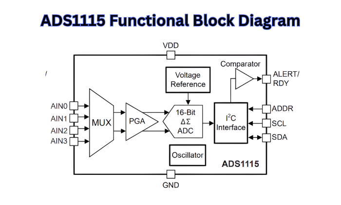
Delta-sigma converters operate by oversampling their input at very high speed while shaping the quantization noise to high frequencies for removal by a digital low-pass filter. This results in a high-resolution digital word being produced at a comparatively low data rate than that of a successive-approximation (SAR) ADC which samples and compares in discrete binary steps.
Key Architectural Advantages
- No sample-and-hold amplifier is necessary because the modulator continuously tracks the input signal
- The noise shaping moves the quantization noise outside of the signal band
- The decimation filter performs a built-in anti-aliasing function
- The differential input topology inherently provides common-mode rejection
Why ΔΣ Outperforms SAR for Precision Sensor Work
SAR ADCs can provide high sampling rates (to tens of megahertz) but the resolution of these devices is limited by the accuracy of the comparators used in them and by the matching of the DAC used to compose the samples.
The maximum resolution for a practical SAR ADC is typically about 18 bits. Delta-Sigma converters compromise throughput to gain high resolution and are traditionally used for instrumentation, medical, and industrial measurements at bandwidths <10 kHz.
Full Electrical Specifications
ADS111x Family Comparison
Texas Instruments offers three devices in the ADS111x family sharing the same pinout. Selecting the correct variant avoids paying for features you do not need.
| Feature | ADS1113 | ADS1114 | ADS1115 ★ |
|---|---|---|---|
| Channels | 1 differential | 1 differential | 4 single-ended / 2 differential |
| Programmable Gain (PGA) | ✕ Fixed ±2.048 V | ✔ 6 settings | ✔ 6 settings |
| Digital Comparator | ✕ No | ✔ Yes | ✔ Yes |
| Input Multiplexer (MUX) | ✕ No | ✕ No | ✔ Yes — 4:1 |
| Resolution | 16-bit | 16-bit | 16-bit |
| Max Data Rate | 860 SPS | 860 SPS | 860 SPS |
| I²C Addresses Available | 1 (fixed 0x48) | 4 | 4 |
| Typical Price (unit) | ~$1.20 | ~$1.40 | ~$1.60 |
ADS1115 vs ADS1015 — Resolution vs Speed Trade-off
The ADS1015 is the 12-bit sibling of the ADS1115 and is pin-for-pin and software-compatible. The choice depends on the application’s primary constraint.
| Parameter | ADS1115 | ADS1015 | Verdict |
|---|---|---|---|
| Resolution | ✔ 16-bit (65,536 steps) | 12-bit (4,096 steps) | 🏆 ADS1115 wins for precision |
| Max Data Rate | 860 SPS | ✔ 3,300 SPS | 🏆 ADS1015 wins for speed |
| Smallest LSB (highest gain) | ✔ 7.8 µV | 125 µV | 🏆 ADS1115: 16× better |
| Typical Use Case |
🌡 Temperature ⚖ Weight 🧪 pH 📏 Strain |
📍 Position 🔊 Audio 💡 Light 🔋 Battery |
Choose by application |
| Library API Compatibility | Adafruit ADS1X15 | Adafruit ADS1X15 | ✔ Drop-in swap |
| Price Premium | ~$0.20–0.40 more | ✔ Lower cost | Minimal difference |
ADS1115 Pinout — Every Pin Explained
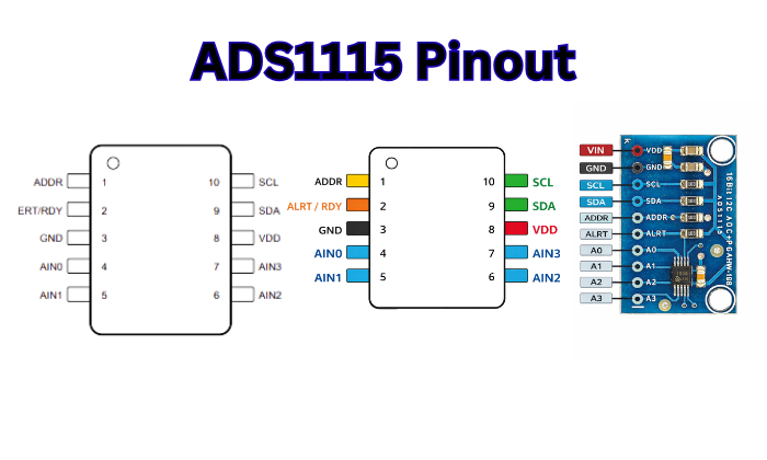
The ADS1115 chip is available in two different package types; specifically, the VSSOP 10-pin and the X2QFN 10-pin package types. The breakout boards provide the same ten allocated pins but label them according to how they are used on the ADS1115 chip. The following pages will discuss: (1) pin functionality, (2) pin wiring requirements, and (3) common wiring mistakes.
| Pin # | Pin Name | Type | Description |
|---|---|---|---|
| 1 | ADDR | ⬇ Input | I²C address select — connect to GND, VDD, SDA, or SCL |
| 2 | ALERT/RDY | ⬆ Output (open-drain) | Comparator output or conversion-ready signal Needs 10kΩ pull-up |
| 3 | GND | ⏚ Power | Ground reference for all signal and logic 0 V reference |
| 4 | AIN0 | 〜 Analog Input | Analog channel 0 — single-ended or differential (+) positive |
| 5 | AIN1 | 〜 Analog Input | Analog channel 1 — single-ended or differential (−) negative |
| 6 | AIN2 | 〜 Analog Input | Analog channel 2 — single-ended or differential (+) positive |
| 7 | AIN3 | 〜 Analog Input | Analog channel 3 — single-ended or differential (−) negative |
| 8 | VDD | ⚡ Power | Positive supply 2.0 V – 5.5 V 3.3 V & 5 V compatible |
| 9 | SDA | ⇅ I²C Data | I²C serial data — bidirectional Needs 4.7kΩ pull-up |
| 10 | SCL | ⬇ I²C Clock | I²C serial clock — input only Needs 4.7kΩ pull-up |

Power Pins: VDD and GND
Supply Voltage and Decoupling
The ADS1115 16-Bit ADC can run from 2 V to 5.5V, so you can use it with either 3.3 V (like Raspberry Pi, ESP32, STM32) or 5 V (e.g. Arduino Uno) without needing to level shift the power rail. The I²C logic level is determined by the VDD — refer to Section 3.3 for information on level shifting.
- Place a 100 nF ceramic capacitor close to the VDD pin; length of leads is important.
- Add a 10 µF bulk electrolytic capacitor at the same supply node
- If you have a breakout board that has a separate AVDD pin, connect both the VDD and AVDD pins to the same supply node unless otherwise directed by the breakout board documentation.
Analog Input Pins: AIN0 – AIN3
Single-Ended Mode
When in single-ended mode, an AIN pin is selected to be measured against GND. The chosen AIN pin connects through the internal MUX to the positive input of the PGA, while GND connects to the negative input of the PGA. The ADC outputs a signed two’s complement value of 16 bits; the effective resolution for single-ended measurements is actually 15 bits of measurement range (0 to +32,767 counts) since the sign bit cannot be used.
| MUX Setting | Positive Input | Negative Input | Typical Use |
|---|---|---|---|
| ▸ Single-Ended Mode — 4 channels | Output range: 0 to +FSR (15-bit effective) | |||
AIN0 / GND
|
+ AIN0 | ⏚ GND | Single-ended channel 0 |
AIN1 / GND
|
+ AIN1 | ⏚ GND | Single-ended channel 1 |
AIN2 / GND
|
+ AIN2 | ⏚ GND | Single-ended channel 2 |
AIN3 / GND
|
+ AIN3 | ⏚ GND | Single-ended channel 3 |
| ▸ Differential Mode — 4 pairs | Output range: ±FSR (full 16-bit signed range) | |||
AIN0 / AIN1
|
+ AIN0 | - AIN1 | Differential pair — bridge sensors |
AIN0 / AIN3
|
+ AIN0 | - AIN3 | Differential pair |
AIN1 / AIN3
|
+ AIN1 | - AIN3 | Differential pair |
AIN2 / AIN3
|
+ AIN2 | - AIN3 | Differential pair — bridge sensors |
Differential Mode
Differential mode measures the voltage differences between two AIN pins. This mode is the best choice for bridge sensors (i.e., strain gauges; load cells; pressure sensors) and long cable runs where common mode noise must be rejected. The full range of ±32,767 counts support the full 16-bit signed resolution.
I²C Bus Pins: SCL and SDA
Pull-up Resistor Requirements
I²C is an open-drain bus — both SDA and SCL require pull-up resistors to VDD. The correct resistor value depends on bus speed and total bus capacitance.
| Bus Speed | Recommended Pull-up | Maximum Bus Capacitance | Notes |
|---|---|---|---|
| 100 kHz Standard mode | 4.7 kΩ | 400 pF | ✔ Default for most breakouts |
| 400 kHz Fast mode | 2.2 kΩ | 400 pF | ⚠ Shorter cable runs only |
| 3.4 MHz High-speed mode | Custom | ~100 pF | Rarely needed for ADS1115 at 860 SPS |
Logic Level Compatibility
Both pins on the ADS1115 are referenced to VDD. With a VDD of 3.3V, as in the case of a Raspberry Pi, you can connect I²C devices without level shifting because the SDA and SCL lines are compatible (3.3V logic). With VDD of 5V, as on Arduino Unos, the SDA and SCL pins are tolerant of 5.0V signals on most Arduinos, however caution must be used when using any microcontroller that is only rated for 3.3V such as an ESP32.
ADDR Pin: Configuring the Four I²C Addresses
The ADDR pin selects one of four I²C device addresses, allowing up to four ADS1115 devices to coexist on a single bus. This provides 16 single-ended channels or 8 differential channels from one MCU I²C port.
| ADDR Pin Connection | I²C Address (7-bit) | Hex | Binary |
|---|---|---|---|
ADDR
→
⏚ GND
|
1001000 | 0x48 | 0100 1000 |
ADDR
→
⚡ VDD
|
1001001 | 0x49 | 0100 1001 |
ADDR
→
⇅ SDA
|
1001010 | 0x4A | 0100 1010 |
ADDR
→
⬇ SCL
|
1001011 | 0x4B | 0100 1011 |
ALERT/RDY Pin: Comparator and Conversion-Ready
Pin Characteristics
ALERT/RDY is an open-drain output that requires an external pull-up resistor (typically 10 kΩ to VDD). It operates in two distinct modes controlled by the Config register.
Comparator Mode
When operating in Comparator Mode, Upon crossing the user-defined threshold set in the Low and High Threshold registers, the comparator pin asserts a Low signal thus allowing the ADS1115 to operate autonomously as an alarm device without the need for any additional firmware polling required by the ADS1115.
| Comparator Mode | Description | Hi_thresh Register | Lo_thresh Register |
|---|---|---|---|
| Traditional |
Asserts ALERT/RDY LOW when result
> Hi_thresh
de-asserts when result
< Lo_thresh
|
⬆ Upper threshold | ⬇ Lower (hysteresis) |
| Window |
Asserts ALERT/RDY LOW when result is
< Lo_thresh
OR
> Hi_thresh
— outside the defined window
|
⬆ Upper boundary | ⬇ Lower boundary |
Lo_thresh = 0x8000 and Hi_thresh = 0x7FFF. Source: Texas Instruments ADS1115 Datasheet SBAS444E.
Conversion-Ready (RDY) Mode
The above implementation is to be enabled by setting both the low threshold of Lo_Thresh to 0x8000 and the high threshold of Hi_Thresh to 0x7FFF. Upon setting these two values to their defined limits, an ALERT/RDY low pulse will occur for one full conversion-length cycle every time new data is ready from the ADC. This enables an interrupt driven method of reading data at full 860 SPS sampling rate without the need for any polling wait period.
Programmable Gain Amplifier (PGA) Configuration
Choosing the PGA for the purposes of measurement accuracy is the most crucial decision that you will make when designing an instrument. By choosing the Full Scale Range of your measurement to match the output of the sensor(s) you are using, you’ll maximize the number of usable Least Significant Bits (LSB) and therefore maximize the effective resolution of your measurement.
PGA Gain Settings and Full-Scale Range
| PGA[2:0] Bits | Full-Scale Range (FSR) | LSB Size | Smallest Measurable Step |
|---|---|---|---|
000
|
±6.144 V | 187.5 µV | Largest range — use for wide-voltage signals |
001
|
±4.096 V | 125.0 µV | Matches 3.3 V single-supply range well |
010
DEFAULT
|
±2.048 V | 62.5 µV | Default on power-up |
011
|
±1.024 V | 31.25 µV | Good for 0–1 V sensors |
100
|
±0.512 V | 15.625 µV | Small signal precision |
101 / 110 / 111
|
±0.256 V | ★ 7.8125 µV | Highest resolution — small differential signals |
Selecting the Optimal Gain for Your Sensor
Matching FSR to Sensor Output
The goal is to choose the smallest FSR that still encompasses the full expected output range of your sensor. A sensor with a 0–100 mV output range should use the ±0.256 V FSR (7.8 µV LSB) rather than the ±4.096 V FSR (125 µV LSB) — the resolution improvement is 16×.
| Sensor Type | Typical Output Range | Recommended FSR | Effective Resolution |
|---|---|---|---|
| 🌡 Thermocouple via AD8495 amp, 5 mV/°C | 0 – 500 mV | ±0.512 V | ~15.6 µV = 0.003 °C step |
| 🌡 PT100 RTD via Wheatstone bridge | −50 to +50 mV differential | ±0.256 V | ★ ~7.8 µV |
| ⚖ Load cell / Strain gauge 10 V excitation | 0 – 30 mV | ±0.256 V | ★ ~7.8 µV = ~0.4 g for 5 kg cell |
| 🌱 Soil moisture resistive divider | 0 – 3.3 V | ±4.096 V | ~125 µV |
| 🕹 Potentiometer / Joystick 0 – 5 V | 0 – 5 V | ±6.144 V ⚠ | ~188 µV ⚠ note AIN safety limit |
| ⚡ Current shunt 10 mΩ, 0–5 A | 0 – 50 mV | ±0.256 V | ★ ~7.8 µV = ~0.78 mA |
| 🔋 Battery voltage 12 V via divider to 3 V | 0 – 3 V | ±4.096 V | ~125 µV |
| 🧪 pH sensor typical conditioned output | 0 – 3.3 V | ±4.096 V | ~125 µV |
Config Register Deep-Dive
Config Register Map (Address 0x01)
The 16-bit Config register controls all operating parameters of the ADS1115 16-Bit ADC. Write it in two bytes (MSB first) over I²C.
| Bits [15:12] | Bits [11:9] | Bits [8:5] | Bits [4:2] | Bits [1:0] |
|---|---|---|---|---|
| OS / MUX[2:0] | PGA[2:0] | MODE / DR[2:0] | COMP_MODE / COMP_POL / COMP_LAT | COMP_QUE[1:0] |
0x01. On power-up default value is 0x8583.
| Field | Bits | Values | Function |
|---|---|---|---|
| OS |
15
|
Write 0 Start conversion
Write 1 No effect Read 0 Conversion in progress Read 1 Device idle |
Single-shot trigger / busy flag |
| MUX[2:0] |
14:12
|
000–111
— see MUX table above
|
Input multiplexer selection |
| PGA[2:0] |
11:9
|
000 = ±6.144 V …
101 = ±0.256 V
|
Programmable gain amplifier |
| MODE |
8
|
0 Continuous conversion
1 Single-shot / power-down |
Conversion mode |
| DR[2:0] |
7:5
|
000 = 8 SPS …
111 = 860 SPS
|
Data rate (samples per second) |
| COMP_MODE |
4
|
0 Traditional comparator
1 Window comparator |
Comparator mode |
| COMP_POL |
3
|
0 Active LOW
1 Active HIGH |
ALERT/RDY polarity |
| COMP_LAT |
2
|
0 Non-latching
1 Latching |
Comparator latch |
| COMP_QUE[1:0] |
1:0
|
00 Assert after 1 conversion
01 Assert after 2 conversions 10 Assert after 4 conversions 11 Disable comparator |
Comparator queue length |
0x8583 — single-shot mode, ±2.048 V FSR, 128 SPS, comparator disabled. Always write the full 16-bit value when configuring. Source: Texas Instruments ADS1115 Datasheet SBAS444E.
Data Rate Register Values
| DR[2:0] | Data Rate (SPS) | Noise Performance | Use Case |
|---|---|---|---|
000
|
8 SPS | ★★★★★ Best Deepest averaging | Maximum precision, static signals |
001
|
16 SPS | ★★★★★ Excellent | DC measurements |
010
|
32 SPS | ★★★★☆ Very good | Low-speed sensors |
011
|
64 SPS | ★★★★☆ Good | General purpose |
100
DEFAULT
|
128 SPS | ★★★☆☆ Standard | Default — balanced |
101
|
250 SPS | ★★★☆☆ Moderate | Faster response needed |
110
|
475 SPS | ★★☆☆☆ Lower | Near real-time monitoring |
111
|
860 SPS ⚡ | ★☆☆☆☆ Lowest Max throughput | Fastest I²C throughput |
Interfacing ADS1115 with Arduino
Hardware Wiring
Arduino Uno and Arduino Mega Pin Connections
| ADS1115 Pin | Arduino Uno | Arduino Mega | Notes |
|---|---|---|---|
| ⚡ VDD | 5V | 5V | Or 3.3V — must match signal levels |
| ⏚ GND | GND | GND | Common ground reference |
| ⬇ SCL | A5 (SCL) | Pin 21 (SCL) | ⚠ Add 4.7 kΩ pull-up to VDD |
| ⇅ SDA | A4 (SDA) | Pin 20 (SDA) | ⚠ Add 4.7 kΩ pull-up to VDD |
| ⬇ ADDR | GND | GND |
Sets I²C address to 0x48
|
| ⬆ ALERT/RDY | Pin 2 (INT0) | Pin 2 (INT0) | Optional 10 kΩ pull-up to VDD required |
| 〜 AIN0–AIN3 | Sensor signal | Sensor signal | ⚠ Must not exceed VDD + 0.3 V |
Reading Single-Ended Channels
Library Installation and Initialisation
Install the Adafruit ADS1X15 library via the Arduino Library Manager (search: “ADS1X15”). This library supports both ADS1015 and ADS1115 with an identical API.
#include <Wire.h>
#include <Adafruit_ADS1X15.h>

Adafruit_ADS1115 ads;  // Default I2C address 0x48

void setup() {
  Serial.begin(115200);
  // Set gain: GAIN_TWOTHIRDS = ±6.144V, GAIN_ONE = ±4.096V,
  // GAIN_TWO = ±2.048V (default), GAIN_FOUR = ±1.024V,
  // GAIN_EIGHT = ±0.512V, GAIN_SIXTEEN = ±0.256V
  ads.setGain(GAIN_ONE);  // ±4.096V FSR
  if (!ads.begin()) {
    Serial.println("ADS1115 not found. Check wiring.");
    while (1);
  }
}

void loop() {
  int16_t raw = ads.readADC_SingleEnded(0);  // Read AIN0
  // Convert to voltage: raw * FSR / 32768
  float voltage = raw * (4.096f / 32768.0f);
  Serial.print("AIN0: "); Serial.print(raw);
  Serial.print(" counts | "); Serial.print(voltage, 4);
  Serial.println(" V");
  delay(500);
}
Reading Differential Channels
// Differential read: AIN0 minus AIN1
// Returns signed int16: range -32768 to +32767
int16_t raw_diff = ads.readADC_Differential_0_1();

// With GAIN_SIXTEEN (FSR = ±0.256V), LSB = 7.8125 µV
float voltage_diff = raw_diff * (0.256f / 32768.0f);
Serial.print("Differential: "); Serial.print(voltage_diff * 1000.0f, 3);
Serial.println(" mV");
Interrupt-Driven Reads Using ALERT/RDY
Configuring the ADS1115 for RDY Mode
Polling the ADS1115 in a tight loop wastes MCU cycles as well as limiting the system’s throughput. Instead, using the ALERT / RDY pin as an interrupt, the MCU can perform other tasks between conversions and ensures that each sample is read at the same output rate as the ADS1115.
volatile bool newDataReady = false;

void IRAM_ATTR rdyISR() {
  newDataReady = true;
}

void setup() {
  Serial.begin(115200);
  ads.setGain(GAIN_ONE);
  ads.begin();

  // Enable RDY mode: set Lo_thresh = 0x8000, Hi_thresh = 0x7FFF
  ads.startADCReading(ADS1X15_REG_CONFIG_MUX_SINGLE_0, true); // continuous
  // Wire ALERT/RDY to MCU INT pin with 10k pull-up
  pinMode(2, INPUT_PULLUP);
  attachInterrupt(digitalPinToInterrupt(2), rdyISR, FALLING);
}

void loop() {
  if (newDataReady) {
    newDataReady = false;
    int16_t raw = ads.getLastConversionResults();
    float v = raw * (4.096f / 32768.0f);
    Serial.println(v, 4);
  }
  // MCU is free to do other work here
}
Interfacing ADS1115 with Raspberry Pi
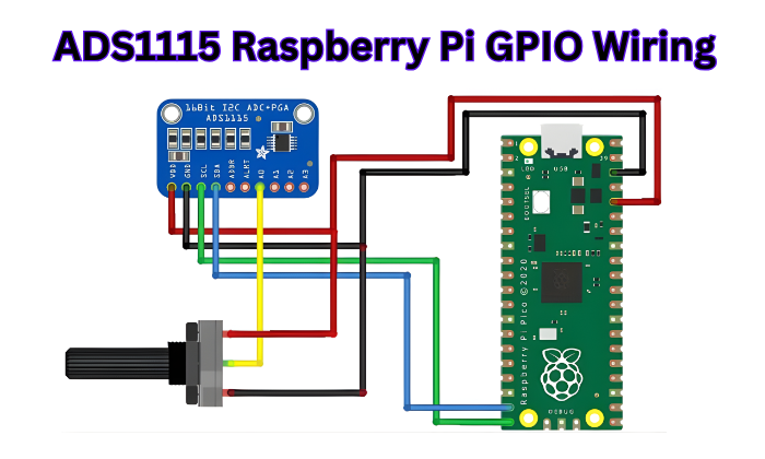
Enabling I²C and Wiring
Raspberry Pi I²C Setup
1. Run sudo raspi-config → Interface Options → I2C → Enable
2. Reboot: sudo reboot
3. Verify detection: sudo i2cdetect -y 1 — ADS1115 should appear at 0x48
4. Install Python library: pip3 install adafruit-circuitpython-ads1x15
| ADS1115 Pin | Raspberry Pi GPIO | Physical Pin | Notes |
|---|---|---|---|
| ⚡ VDD | 3.3V | Pin 1 | 3.3 V logic Raspberry Pi is 3.3 V — no level shifter needed |
| ⏚ GND | GND | Pin 6 | Common ground reference |
| ⬇ SCL | GPIO3 (SCL1) | Pin 5 | ✔ Internal 1.8 kΩ pull-up to 3.3 V — no external resistor needed |
| ⇅ SDA | GPIO2 (SDA1) | Pin 3 | ✔ Internal 1.8 kΩ pull-up to 3.3 V — no external resistor needed |
| ⬇ ADDR | GND | Pin 9 |
Sets I²C address to 0x48
|
| ⬆ ALERT/RDY | GPIO17 | Pin 11 | Optional ⚠ 10 kΩ pull-up required For interrupt-driven reads |
sudo raspi-config → Interface Options → I2C before use. Source: Texas Instruments ADS1115 Datasheet SBAS444E.
Python Code with CircuitPython ADS1x15 Library
import board
import busio
import adafruit_ads1x15.ads1115 as ADS
from adafruit_ads1x15.analog_in import AnalogIn

# Initialise I2C bus and ADS1115
i2c = busio.I2C(board.SCL, board.SDA)
ads = ADS.ADS1115(i2c)        	# Address 0x48 by default
ads.gain = 1                   	# GAIN_ONE = ±4.096 V FSR

# Single-ended channel reads
ch0 = AnalogIn(ads, ADS.P0)   	# AIN0 vs GND
ch1 = AnalogIn(ads, ADS.P1)   	# AIN1 vs GND

print(f"AIN0: {ch0.value} counts | {ch0.voltage:.4f} V")
print(f"AIN1: {ch1.value} counts | {ch1.voltage:.4f} V")

# Differential read: AIN0 minus AIN1
ch_diff = AnalogIn(ads, ADS.P0, ADS.P1)
print(f"Differential: {ch_diff.voltage*1000:.3f} mV")
Connecting Multiple ADS1115 Devices on One I²C Bus
Instantiating Multiple Devices in Python
import board, busio
import adafruit_ads1x15.ads1115 as ADS
from adafruit_ads1x15.analog_in import AnalogIn

i2c = busio.I2C(board.SCL, board.SDA)

# Device 1: ADDR → GND  →  0x48
ads_a = ADS.ADS1115(i2c, address=0x48)
# Device 2: ADDR → VDD  →  0x49
ads_b = ADS.ADS1115(i2c, address=0x49)
# Device 3: ADDR → SDA  →  0x4A
ads_c = ADS.ADS1115(i2c, address=0x4A)
# Device 4: ADDR → SCL  →  0x4B
ads_d = ADS.ADS1115(i2c, address=0x4B)

# Now read all 16 single-ended channels
devices = [ads_a, ads_b, ads_c, ads_d]
for dev_idx, dev in enumerate(devices):
    for ch_idx in [ADS.P0, ADS.P1, ADS.P2, ADS.P3]:
        ch = AnalogIn(dev, ch_idx)
        label = f"Dev{dev_idx+1}_AIN{ch_idx}"
        print(f"{label}: {ch.voltage:.4f} V")
High-Resolution Sensor Interfacing: Practical Examples
Temperature Measurement via Thermocouple Amplifier
Circuit: Type-K Thermocouple + AD8495 + ADS1115
The AD8495 is a precision thermocouple amplifier that outputs 5 mV/°C with internal cold-junction compensation. This voltage is well-suited for the ADS1115 with the ±0.512 V PGA setting.
| Parameter | Value | Notes |
|---|---|---|
| AD8495 output sensitivity | 5 mV / °C | 0 V at 0 °C with proper biasing |
| Measurement range ±0.512 V FSR | −102 °C to +102 °C | Before external biasing |
| ADS1115 LSB at ±0.512 V FSR | 15.625 µV | ★ 0.003 °C per step |
| Required PGA setting | GAIN_EIGHT ±0.512 V FSR |
ads.setGain(GAIN_EIGHT)
|
| AD8495 supply voltage | 2.7 V – 5.5 V | ⚠ Match ADS1115 VDD |
Strain Gauge / Wheatstone Bridge (Differential Mode)
Specifically, when using a stable voltage source, a Wheatstone bridge produces a small output voltage that varies based on the amount of strain applied. To illustrate, a bridge powered with a 5 V excitation and a 10 kΩ strain gauge may produce an output in the range of 1 mV to 5 mV, depending on the measurement conditions. For this reason, the ADS1115’s differential input is well-suited for handling these small signals due to its built-in programmable gain amplifier (PGA), which allows accurate measurement of low-level voltages.
Noise Averaging Strategy
// 64-sample averaging to reduce noise floor by ~8x (1/sqrt(64))
const int NUM_SAMPLES = 64;
long sum = 0;
for (int i = 0; i < NUM_SAMPLES; i++) {
    sum += ads.readADC_Differential_0_1();
    delay(1);  // ~1 ms between samples at 860 SPS
}
int16_t averaged = (int16_t)(sum / NUM_SAMPLES);
float grams = (float)averaged * GRAMS_PER_COUNT;  // calibrate GRAMS_PER_COUNT
Current Sensing with a Shunt Resistor
Low-Side Current Measurement
Connect a low-resistance shunt resistor (10 mΩ – 100 mΩ) in series with the load return path. Measure the differential voltage across the shunt with the ADS1115 16-Bit ADC AIN0/AIN1 differential input and the ±0.256 V PGA setting.
| Shunt Resistance | Max Current (±256 mV FSR) | Current Resolution (7.8 µV LSB) | Power Dissipation at Max |
|---|---|---|---|
| 10 mΩ | 25.6 A | 0.78 mA | 6.6 W ⚠ Heatsink required |
| 50 mΩ | 5.12 A | 0.156 mA | 1.3 W |
| 100 mΩ | 2.56 A | 78 µA | 0.66 W |
| 500 mΩ | 512 mA | ★ 15.6 µA | 0.13 W ★ High precision |
Battery Voltage Monitoring with Resistor Divider
For voltages above VDD, a resistor divider scales the battery voltage to within the ADS1115 input range. Use precision 0.1% resistors to maintain the accuracy the 16-bit ADC provides.
| Battery Type | Max Voltage | R1 (top) | R2 (bottom) | Scaled Max Voltage | Recommended FSR |
|---|---|---|---|---|---|
| 🔋 4S LiPo | 16.8 V | 560 kΩ | 100 kΩ | 2.55 V | ±4.096 V |
| 🔋 12 V Lead Acid | 14.4 V | 390 kΩ | 100 kΩ | 2.94 V | ±4.096 V |
| 🔋 24 V Li-ion pack | 29.4 V | 820 kΩ | 100 kΩ | 3.16 V | ±4.096 V |
Noise, Accuracy, and Signal Integrity
Effective Resolution vs Nominal Resolution
The ADS1115 is a 16-bit ADC. Realistically, the effective number of bits (ENOB), for a certain data rate and environment (e.g. the PCB), will vary. For example, if you had an ADS1115 with a data rate of 860 SPS in a typical prototype environment, you would typically get around 14-15 ENOB. However, if you reduce the data rate to 8 SPS (the max decimation filter depth), it is possible to achieve an ENOB up to approximately 15.5.
| Data Rate | Approximate ENOB | Noise (µV rms, ±2.048 V FSR) | Best Application |
|---|---|---|---|
| 860 SPS ⚡ |
~14.0 ENOB
|
~100 µV rms | Real-time monitoring, waveform capture |
| 128 SPS DEFAULT |
~14.8 ENOB
|
~40 µV rms | General sensor polling |
| 32 SPS |
~15.2 ENOB
|
~20 µV rms | Precision measurements |
| ★ 8 SPS |
★ ~15.5 ENOB
|
★ ~11 µV rms | Maximum precision, static signals only |
PCB Layout Best Practices
Critical Layout Rules
- Place a 100 nF (X7R) ceramic decoupling capacitor as close as possible (within 2 mm) to the VDD pin.
- Add a 10 µF bulk capacitor (either tantalum or electrolytic) at the point where power enters the ADS1115 circuit.
- Keep the AIN traces as short as possible. Every millimeter contributes approximately 1 pF of capacitance (the longer the trace, the higher the capacitance).
- Do not route any digital signals (e.g., SDA, SCL, PWM, clock lines) in parallel with the AIN traces.
- Mount the ADS1115 16-Bit ADC close to the connector for the sensor and away from any switching voltage regulator.
- Use a solid analogue ground plane below the ADS1115, connecting to the digital ground plane at a single point only.
- For high-impedance source AINs (> 10 kΩ), place a 100 nF capacitor between AIN and GND to filter out RF interference
Software Noise Reduction Strategies
| Technique | Noise Reduction | Latency Impact | Code Complexity | When to Use |
|---|---|---|---|---|
| N-sample averaging | 1/√N factor | N × sample period | Low | Most general-purpose measurements |
| Exponential moving average (EMA) | Configurable | Continuous, rolling | Low | Real-time streaming with slow variation |
| Median filter (N samples) | Spike / glitch rejection | N × sample period | Medium | EMI-prone environments, transient loads |
| Boxcar (rectangular window) | 1/√N factor | N samples | Low | When equal weighting is required |
| Reduce data rate (hardware — try first) | ★ Deep digital filtering | Higher delay | ★ None | ★ Always try first Free improvement — no code required |
Troubleshooting Common Issues
| Symptom | Likely Cause | Solution |
|---|---|---|
I²C
i2cdetect shows no device
|
⚠ Wiring
Missing pull-ups or wrong address |
Check 4.7 kΩ pull-ups on SDA/SCL; verify ADDR pin connection
sudo i2cdetect -y 1
|
Code
ads.begin() returns false
|
⚠ Address
I²C address mismatch |
Pass correct address to constructor:
Adafruit_ADS1115 ads(0x49);
|
|
Readings
Stuck at 32767 or −32768
|
⚠ Overvoltage
Input voltage exceeds FSR or AIN > VDD |
Reduce PGA FSR or add voltage divider; check absolute max rating
Max AIN = VDD + 0.3 V
|
|
Readings
Reading shows −1 or 0 always
|
⚠ Wiring
SDA/SCL reversed or floating |
Verify wiring; check pull-up resistors; run i2cdetect to confirm bus activity
|
|
Expected
Only 15-bit range in single-ended mode |
✔ Normal behaviour
Sign bit is reserved |
Range is 0 to +32,767 in single-ended. Use differential mode for full ±32,767 signed range
readADC_Differential_0_1()
|
|
Noise
High noise on readings |
⚠ PCB / Supply
Supply noise or long AIN traces |
Add decoupling caps; shorten AIN traces; reduce data rate; use software averaging |
|
Accuracy
Readings drift with temperature |
⚠ Calibration
No reference calibration applied |
Implement two-point calibration with known reference voltages at operating temperature |
|
Multi-device
Multiple devices return same reading |
⚠ ADDR pin
ADDR pin not properly connected |
Verify each ADDR pin connection is secure; check for shorts between pads
Addresses: 0x48 0x49 0x4A 0x4B
|
|
Interrupt
ALERT/RDY pin never asserts |
⚠ Config
Pull-up missing or comparator not configured |
Add 10 kΩ pull-up to VDD; verify
Hi_thresh /
Lo_thresh register values
|
|
ESP32
Values correct but ESP32 I²C errors |
⚠ Logic level
3.3 V logic but 5 V ADS1115 VDD |
Power ADS1115 from 3.3 V when connecting to ESP32; add level shifter if 5 V supply is required
ESP32 SDA → GPIO21 | SCL → GPIO22
|
Conclusion: When to Use the ADS1115
Summary Decision Matrix
| Requirement | ADS1115 Suitable? | Recommended Alternative | Reason |
|---|---|---|---|
| 16-bit precision, low speed < 860 SPS | ✔ Yes — ideal | — | ★ Purpose-built Purpose-built for this use case |
| 12-bit sufficient, need > 1 kSPS | ✕ No | ADS1015 | 4× faster at 3,300 SPS — same Adafruit API, drop-in swap |
| Need SPI interface | ✕ No | MCP3208 ADS8688 | ADS1115 is I²C only — no SPI mode available |
| Need > 4 channels without cascading | ✕ No | ADS1115 × 2 ADS131M08 | Max 4 single-ended channels per chip — cascade up to 4 devices for 16 channels |
| Weight / load cell measurement | ✔ Yes — excellent | HX711 (dedicated) | ADS1115 more flexible — measures any sensor type, not just load cells |
| Current sensing < 100 mA precision | ✔ Yes | INA219 INA226 | Either works — INA219/226 simpler for current-only; ADS1115 better for multi-sensor designs |
| Temperature (thermocouple) | ✔ Yes — with amp | MAX31855 (simpler) | ADS1115 more general-purpose — use with AD8495 amp for any thermocouple type |
| Battery voltage monitoring | ✔ Yes — with divider | — | High accuracy SoC estimation — 16-bit resolution gives precise voltage readings |
| Audio signal capture | ✕ No | PCM1808 CS5343 |
860 SPS max << minimum audio bandwidth (8,000 SPS)
Not suitable for audio
|
Key Takeaways
- The ADS1115 outputs 16-bits of resolution up to 860 samples per second from a 2-5.5V power supply via I²C
- The PGA FSR should always be selected to match your sensor’s output range for maximum effective bits.
- Bridge sensors should be connected to the ADS1115 in a differential mode because single ended mode will lose the sign bit (i.e. the 15th bit).
- A maximum of four ADS1115 devices can be connected together with an I²C bus because they share the ADDR pin for a total of 16 channels.
- Increase real-world ENOB and analog performance by decreasing the sample rate, increasing the decoupling capacitors, and implementing software averaging of multiple samples.
- The Adafruit ADS1X15 Arduino and CircuitPython libraries use the same API for both platforms, making it easier to migrate from one platform to another.
Frequently Asked Questions
In differential mode, the device can measure negative voltages as low as -FSR, provided that neither of the AIN pins goes below -0.3V with respect to GND. Device is unable to measure negative voltages in single-ended mode
The device will only input positive values (0 to 32767) into memory when coding in single-ended mode and will reserve the sign bit for differential voltage measurements.
In any case, the maximum input to the device will be VDD + 0.3V and the minimum input will be -0.3V, irrespective of the setting on the PGA. For example, if it receives a supply of 3.3V, the maximum voltage allowed is 3.6V.
Power it with 3.3 V and connect via I²C (ESP32: GPIO21/22, ESP8266: GPIO4/5). Use the Adafruit ADS1X15 library and initialize with Wire.begin().
Up to 4 devices (addresses 0x48–0x4B), giving 16 single-ended or 8 differential channels.
Continuous mode updates readings continuously. Single-shot mode takes one reading and enters low-power sleep, making it ideal for battery-powered systems.

COMMENTS