Indoor photovoltaic (IPV) systems, harnessing solar energy within enclosed spaces, are pivotal for powering Internet of Things (IoT) devices. However, the transition from traditional outdoor solar applications to indoor environments presents unique challenges.
What Are the Primary Challenges of Indoor Solar Cells?
Indoor solar cells are designed to capture ambient light, such as that emitted by LED bulbs. However, the intensity and spectrum of indoor lighting differ significantly from natural sunlight, affecting the efficiency of these cells.
Why Is Standardization Crucial for Indoor Photovoltaics?
The absence of standardized testing protocols for indoor photovoltaic systems leads to inconsistencies in performance evaluation. Developing standardized methods is essential for comparing different technologies and ensuring reliable performance across various indoor environments.
How Do Different Light Sources Affect Solar Cell Performance?
Indoor lighting sources, including LEDs with varying color temperatures, emit light spectra distinct from natural sunlight. These differences necessitate the development of solar cells tailored to efficiently convert indoor light into electricity.
What Materials Are Promising for Indoor Solar Cells?
Materials such as organic photovoltaics (OPVs), perovskite solar cells, and amorphous silicon are being explored for indoor applications due to their ability to operate effectively under low-light conditions. Each material offers unique advantages in terms of efficiency and adaptability to indoor lighting.
How Can Energy Harvesting Be Optimized in Indoor Settings?
Optimizing energy harvesting involves selecting appropriate materials and designing solar cells that maximize efficiency under indoor lighting conditions. This includes considering factors like spectral matching and the geometry of the solar cell to enhance light absorption.
Why Is Long-Term Stability Important for Indoor Solar Cells?
Indoor solar cells must maintain consistent performance over extended periods, despite exposure to fluctuating light conditions. Ensuring long-term stability is crucial for the reliability of IoT devices powered by these cells.
How Do Environmental Factors Influence Solar Cell Efficiency?
Factors such as temperature, humidity, and dust accumulation can impact the efficiency of indoor solar cells. Designing systems that mitigate these effects is essential for maintaining optimal performance.
What Are the Future Prospects for Indoor Photovoltaics?
Advancements in materials science and photovoltaic technology hold promise for enhancing the efficiency and applicability of indoor solar cells. Continued research and development are expected to lead to more effective solutions for powering IoT devices in indoor environments.
Buying Tips
When selecting indoor photovoltaic systems for IoT applications, consider factors such as efficiency under low-light conditions, material durability, and compatibility with existing IoT devices. It’s advisable to consult with suppliers who specialize in indoor solar technologies to ensure the best fit for your specific needs.
Electronic Components Expert Views
The integration of indoor photovoltaic systems into IoT applications represents a significant step towards sustainable technology. However, addressing the challenges related to light spectrum compatibility and standardization is essential for widespread adoption.”
FAQ
Q: Can indoor solar cells power IoT devices effectively?
A: Yes, indoor solar cells can power IoT devices, but their efficiency depends on factors like light intensity and spectrum.
Q: What materials are best suited for indoor solar cells?
A: Materials such as OPVs, perovskite, and amorphous silicon are promising for indoor applications due to their performance under low-light conditions.
Q: Why is standardization important for indoor photovoltaics?
A: Standardization ensures consistent performance evaluation, facilitating the comparison and development of indoor photovoltaic technologies.
Indoor lighting differs significantly in both intensity and spectrum from natural sunlight, which means indoor photovoltaic (IPV) technology must be tailored accordingly. This article explores the unique challenges of IPV cells, along with potential solutions, testing methodologies, and applicable standards.
The Internet of Things (IoT) market is rapidly expanding, with a wide range of applications, from smart home systems to industrial sensors. If this trend continues, billions of low-power devices will need to be deployed, many of them within buildings.
While substantial research has focused on reducing the power consumption of these devices, finding efficient solutions for powering these billions of units remains a critical challenge. IoT has the potential to save up to 1.6 petawatt-hours of energy annually through smart energy management, heating systems, and more. However, the proliferation of IoT devices will also increase global energy demand by an estimated 34 terawatt-hours.
Most individual sensors are currently battery-powered, but relying on disposable batteries introduces its own set of challenges. Frequent battery replacements can be wasteful, time-consuming, and inefficient. Additionally, IoT technology is ideally designed to operate autonomously, monitoring and controlling environments without human intervention—something that becomes less feasible if batteries need to be replaced regularly.
Using Indoor PVs for IoT Applications
Indoor photovoltaics (IPV) present a compelling option for powering individual sensors and nodes. As their name implies, IPV systems are specifically engineered to harness indoor lighting efficiently. Over traditional batteries, IPV offers several advantages:
- Extended Lifespan: Ensuring long-term, reliable operation without the need for frequent replacements.
- Minimized Human Intervention: Reducing the dependency on manual maintenance and replacements.
- Lower Waste Generation: Contributing to a more sustainable environment by minimizing electronic waste.
- Enhanced Energy Efficiency: Maximizing the utilization of indoor light for power generation.
- Higher Self-Sufficiency: Enabling devices to operate autonomously, reducing the reliance on external power sources.
Figure 1 illustrates the surge in research dedicated to IPV devices, which has grown annually in tandem with the expanding IoT market, highlighting the burgeoning potential of the IPV industry.
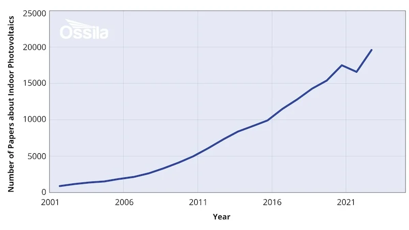
Figure 1. Number of papers published per year linked to the keywords: indoor photovoltaics. Data collected from Google Scholar by Ossila.
The IPV market is expected to exceed 1 billion USD by 2030. This highlights the importance of optimizing and developing efficient IPV technologies to reduce both environmental and financial costs.
Designing Indoor vs. Outdoor PV
Outdoor solar cells undergo rigorous testing under standardized conditions using the AM 1.5G spectrum, which simulates sunlight with an irradiance of 1000W/m2. These controlled tests generally provide an accurate indication of how solar cells will perform under direct sunlight.
Conversely, indoor lighting presents a far more variable environment. The myriad types of indoor lighting—such as warm LED, cool LED, and fluorescent bulbs—share a common trait: their light distribution primarily falls within the visible spectrum, unlike sunlight.
This fundamental distinction necessitates a different approach when designing solar panels for indoor versus outdoor applications, particularly in terms of their ideal band gaps.
The ideal band gap for solar panels is the sweet spot where the maximum electrical energy can be extracted from the incident light. In essence:
- A lower band gap material absorbs more light, thereby generating higher currents.
- A higher band gap material converts this absorbed light into greater voltages.
Achieving optimal power extraction necessitates a delicate balance between these two factors, requiring the PV material to closely align with its ideal band gap. For outdoor solar panels, the ideal band gap is approximately 1.34 eV. However, indoor photovoltaic (IPV) cells typically have a significantly higher ideal band gap ranging from 1.8 to 1.9 eV. To create high-efficiency IPV devices, it is imperative to select materials with band gaps near 1.9 eV.
Furthermore, indoor light sources generally exhibit much lower intensities compared to sunlight. While solar irradiation measures 1000 W/m2, an indoor LED white light source may only have a luminosity of 500 lux, equivalent to roughly 1.5W/m2. Consequently, IPV cells must be capable of operating efficiently even in these dimmer conditions.
C-Si Solar Panels for IPV?
Crystalline-silicon (c-Si) photovoltaic technology stands as the predominant choice for outdoor solar panels. With a band gap ranging from 1.1 to 1.2 eV, silicon-based solar panels are theoretically capable of absorbing all incoming sunlight below the 1100 nanometer wavelength, thereby enhancing the available current (as illustrated in Figure 2). This characteristic is particularly advantageous for outdoor PV systems, as the solar spectrum extends considerably into the infrared region.
However, there is a compromise to be made: the voltage generated by c-Si solar panels is inherently limited. For outdoor applications, this voltage loss is mitigated by the substantial increase in current, enabling c-Si solar panels to attain reasonably high efficiencies despite this limitation.
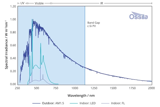
Figure 2. Comparison of the silicon band gap to the spectral distribution of sunlight (AM 1.5), an LED light source, and a fluorescent light source.
Nonetheless, the spectral distribution of indoor light sources does not extend into the non-visible spectral regions; there is no inherent reason for it to do so. Consequently, when crystalline silicon (c-Si) is utilized in indoor photovoltaic (IPV) applications, a reduced voltage is generated due to the absence of enhanced absorption or increased current in the non-visible ranges. This ultimately results in IPV devices exhibiting lower efficiencies. Figure 3 provides a clear illustration of the optimal band gap for IPV applications.
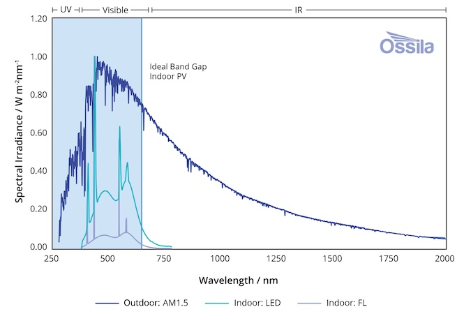
Figure 3. The ideal band gap for indoor photovoltaics, with the spectral distribution of sunlight (AM 1.5G), an LED light source, and a fluorescent light source.
Another notable issue with crystalline silicon photovoltaic (c-Si PV) technology is its suboptimal performance under lower light intensities. At higher light intensities, equivalent to 1000W/m2 (or 1 Sun), any imperfections that could hinder device performance, such as light traps, are overshadowed by the abundant incoming light. However, in environments with low light intensities, loss mechanisms become more prominent, and device short-circuiting becomes a frequent occurrence. As a result, the efficiency of commercially available c-Si solar panels decreases from 15% in high light conditions to just 5% in low light intensities (approximately 700 lux).
Furthermore, to ensure efficiency, silicon solar panels must be constructed with a considerable thickness, rigidity, and weight, which poses limitations on their applicability in Internet of Things (IoT) devices. These constraints suggest that alternatives to silicon solar cells may offer more suitable solutions for indoor environments.
Other PV Technologies for Indoor PV Applications
Third-generation photovoltaic technologies, such as organic solar cells (OSCs) and perovskite solar cells (PSCs), emerge as promising contenders for indoor photovoltaic (IPV) applications.
They offer several key advantages:
- Tuneable Band Gaps: By altering the composition of perovskite materials or the types of organic materials utilized, the band gap can be tailored to align with indoor light sources, thereby enhancing efficiency.
- Solution-Processible: Both OSCs and PSCs are primarily processed through solution-based methods. Although certain air-sensitive components may necessitate controlled deposition environments, such as a glove box, this process is significantly less energy-intensive and resource-consuming compared to silicon solar cell production.
- Thin, Flexible Devices: Simpler processing techniques and thin active layers facilitate the deposition of OSCs and PSCs onto a diverse range of substrates, including polymer substrates for flexible devices or curved surfaces.
- Lower Manufacturing Costs: Solution-processing methods have the potential to reduce manufacturing costs, which is crucial for making IoT nodes affordable.
- Excellent Performance at Low Light Intensities: Both PSCs and OSCs demonstrate impressive performance under low light conditions. Perovskite materials exhibit low defect tolerance, minimizing loss mechanisms compared to c-Si PV. For instance, PSCs have achieved a power conversion efficiency of 45% in indoor light conditions using a wide band gap perovskite.
OSC devices also shine under low light intensities due to their high shunt resistance. A PM6:Y6 OSC blend solar cell has accomplished a power conversion efficiency of approximately 32% under LED illumination.
Despite their promising potential, both OSCs and PSCs confront challenges related to stability, as they are susceptible to degradation from environmental factors such as heat, moisture, and oxygen. Inert processing and adequate encapsulation can alleviate these issues, but further advancements are essential for large-scale production.
Standardising Indoor Light PV Testing
One of the foremost hurdles in the development of indoor photovoltaic (IPV) systems lies in the absence of standardized testing protocols. This stems primarily from the vast variability in both spectral distribution and intensity among indoor lighting sources.
As previously discussed, the AM 1.5G spectrum is meticulously defined, and solar simulators are designed to closely replicate this spectrum. Consequently, numerous standards have been established to specify the precise light sources required for testing outdoor solar cells (such as ASTM E927-19, IEC 60904-9:2020, and JIS C 8904-9).
In 2023, the IEC introduced Technical Specification 62607-7-2, which outlines methodologies for testing solar cells under indoor lighting conditions. However, this specification does not rigidly define a spectral distribution.
The complexity of testing indoor PVs is compounded by the fact that indoor light is measured in terms of luminosity, which reflects how light is perceived by the human eye, whereas outdoor testing employs illuminance, which quantifies the light’s power over a specified area. This discrepancy poses challenges in establishing a coherent testing protocol.
While the introduction of some standards represents progress, further efforts are imperative to develop precise standards for the testing and performance evaluation of indoor PVs. The establishment of such standards will be pivotal in ensuring the consistent and reliable performance of IPV technologies across the industry.