
The Avalanche Photodiode (APD) is a semiconductor photodetector that has built-in signal amplification capabilities based on impact ionization mechanisms. In this detailed article, we’ll see what an APD actually is, how it works, including its operating mechanism (impact ionization, multiplication, various layers in the device, its gain, and noise), and biasing methods for the reverse bias mechanism. The reverse bias mechanism plays a crucial role in the APD’s gain achievement.
For understanding the performance of the avalanche photodiode, we’ll also look at control parameters such as gain, bandwidth, material, noise, and sensitivity of the APD. Finally, we’ll see some actual APD products from various manufacturers and their key performance parameters extracted from respective avalanche photodiode datasheets.
For understanding the performance of the avalanche photodiode, we’ll also look at control parameters such as gain, bandwidth, material, noise, and sensitivity of the APD. Finally, we’ll see some actual APD products from various manufacturers and their key performance parameters extracted from respective avalanche photodiode datasheets.
Avalanche Photodiode Basics
In simplest terms, an avalanche photodiode is a light-sensitive electronic device that generates an electrical current when it detects light. However, a lot goes into its operational side to make it work like that.
Avalanche Photodiode
An avalanche photodiode is a specialized photodiode that operates on an impact ionization mechanism based on reverse bias. In this mechanism, the photodiode is under high reverse bias so much so that a single photon triggers a cascade of ionization events called ‘avalanche’. This avalanche produces an amplified current, usually regarded as the gain. Without impact ionization, even with external amplification, this weak signal could otherwise be lost; however, the avalanche mechanism successfully detects it through impact ionization.
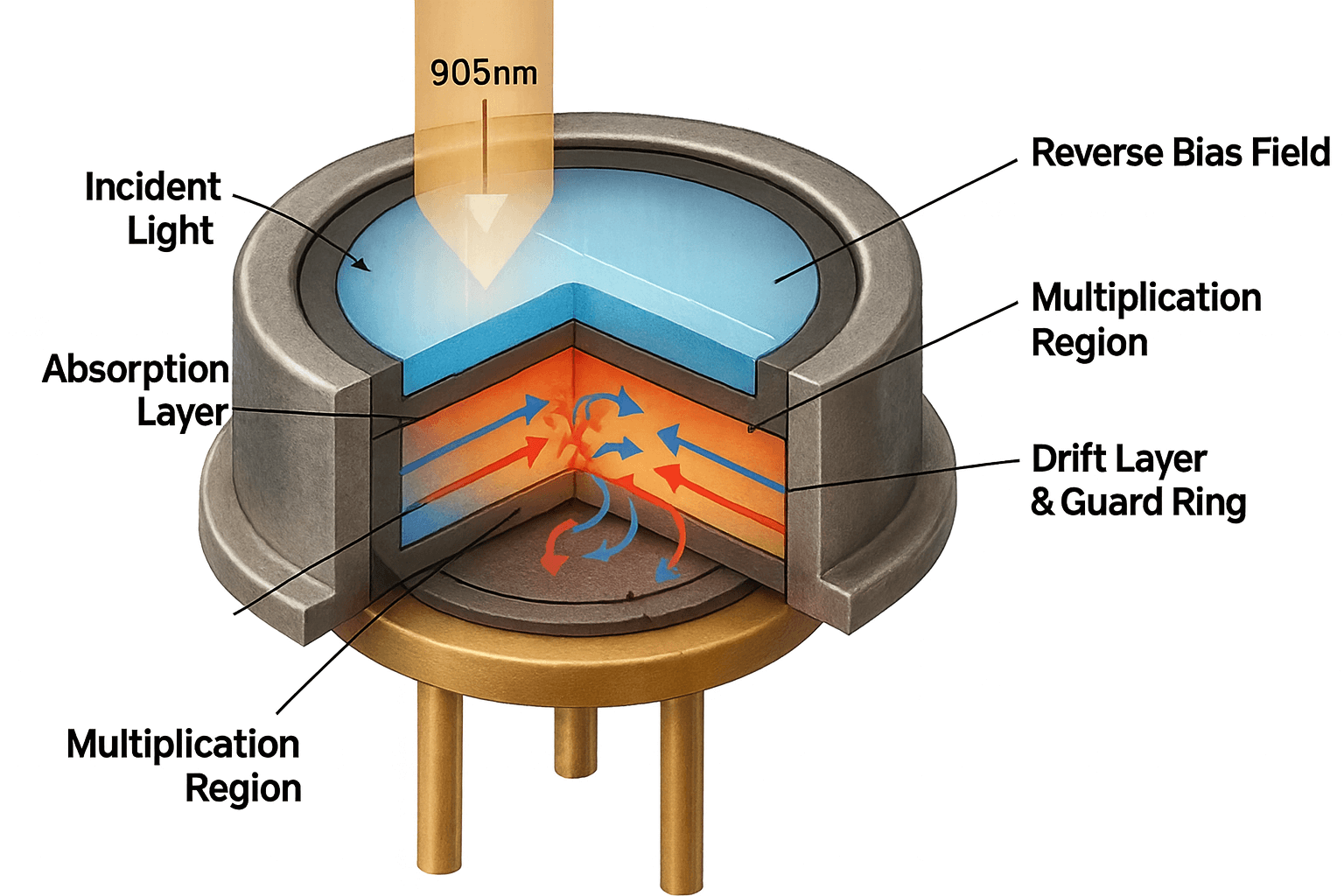
Let’s look at how this impact ionization works since it is the backbone of the APD operation. When you apply a high reverse bias voltage, keeping it under the breakdown voltage, even a single photon of light can generate an electron–hole pair. That carrier accelerates in the strong electric field, collides and creates secondary carriers, and so on, multiplying (amplifying) the current.
APDs vs PMTs
From an operational point of view, the avalanche photodiodes work just like the photomultiplier tubes (PMTs). However, the APDs are analog versions of the PMT and are compact, solid-state packages compared to PMTs.
Avalanche Photodiode Construction & Materials
The internal APD structure consists of two main regions:
An APD’s Absorption Region is where the photons generate carriers (by knocking out the electrons) and
A Multiplication Region where the carriers are accelerated under a strong electric field. The operational performance of the APD depends upon the design of these two regions, particularly the high-electric field zone for avalanche multiplication
Material and Design of Avalanche Photodiode
You can make APD semiconductors using one of two main types of materials, and the selection of material also selects the bandwidth of their operation:
Silicon Avalanche Photodiode (Si APD)
The APDs built using Si (Silicon) material are most common. They cover the wavelengths of light in the visible to near-infrared (IR) region (up to 1100 nm), and without any excessive noise in gain. The Si-APDs are particularly useful in LiDAR, optical communication, and medical imaging.
InGaAs Avalanche Photodiode
The InGaAs (Indium Gallium Arsenide) is another material widely used to make avalanche photodiodes. The APDs built using InGaAs can cover the wavelength range between 900–1700 nm. They are better suited for optical fiber systems and telecommunications. These APDs, however, require heterostructure design to manage noise.
Large Area Avalanche Photodiode
Some applications require a larger area of avalanche photodiode to collect more photons or to enable the APD to accept a divergent beam. This large area does come with a caveat. Increasing the area increases capacitance, which downgrades the coverage bandwidth and increases noise. So there’s a trade-off between sensitivity vs speed when choosing the APD area.
Avalanche Photodiode Device Structure
The APD device has a complex structure that includes multiple layers constructed using distinct materials. Further, the layers are arranged in numerous configurations depending upon the bandwidth coverage, target device gain, and performance, as we see below.
Separate Absorption, Multiplication (SAM) Structure
Common APDs use distinct materials for various functions. For example, the InGaAs layer is used for light absorption, and the InP layer for carrier multiplication. Splitting these processes into distinct layers allows fine-tuning the electric field and doping profile in each region independently, eventually improving both sensitivity and speed.
APD Reach-through Configuration
This configuration has an extended absorption layer above a deeper multiplication region. The depletion zone connects both regions, allowing efficient carrier collection. Advances in APD engineering include engineered impact ionization and staircase structures to reduce excess noise and improve gain–bandwidth product. An example of such a configuration is explained in research on the Near-unity excess noise factor in staircase avalanche photodiodes has shown that specialized structures can reduce noise substantially at moderate gains.
Avalanche Photodiode Operating Mechanisms
Reverse Bias and Impact Ionization
For an APD to function, a high reverse bias voltage is applied that brings the device close to, but below its breakdown voltage. In this high electric field region, carriers gain significant kinetic energy to cause impact ionization, subsequently generating secondary electron–hole pairs. This chain reaction is what gives the APD its internal gain.
APD Gain, Sensitivity, and Bandwidth
The factors, such as the strength of the electric field and impact ionization, are of a stochastic nature, and Nonlocal models and Monte Carlo simulations help predict gain and noise behavior.
Avalanche Photodiode Gain
The Gain (M) of an APD is a key metric. Practically, APDs operate at moderate gains (e.g., 20–200) to balance signal amplification and noise production. If aimed at higher gains, the noise and breakdown instability become the most probable risk. There is an analytical formula to model the mean gain, and excess noise F(M) as given below:
$$F(M)=kM+(2-\frac{1}{M})(1-k)$$
Where ‘k’ is the ratio of ionization coefficients
Bandwidth & Rise Time
In APD design, a fundamental trade-off is between the gain and speed. As a PAD gain increases, the effective bandwidth decreases since the avalanche process takes more time, and the device capacitance interacts with circuit elements. Therefore, a design choice must be made to choose a gain such that the target bandwidth is preserved.
Noise Sources and SNR
As described earlier, achieving better gain in an avalanche photodiode involves a substantial risk of increasing noise. Here we’ll see what kind of noises are involved, adding to the total noise in the APD device:
- Excess and Shot Noise: The main internal noise sources in an APD are shot noise and excess noise. Shot noise arises from the random photon arrivals governed by Poisson statistics, while excess noise results from the stochastic nature of avalanche multiplication—also known as multiplication noise. Together, these gain fluctuations degrade the signal-to-noise ratio (SNR). The excess noise factor F(M) increases with gain M, limiting the maximum usable APD gain.
- Dark Current: Dark current occurs when carriers are produced not due to photon impact, but because of temperature. This thermal noise in APD (because it is not produced due to photon detection) contributes to shot noise, adding parallel noise. It is therefore critical to lower the dark current via cooling or design choice.
- 1/f and Flicker Noise: Low-frequency (1/f) noise, caused by carrier trapping and release at defects, adds slow current fluctuations that add to the noise floor. Low-frequency noise can add to overall SNR degradation. Clean fabrication and stable biasing are vital to minimizing these effects and ensuring APD reliability.
APD Device Types & Operating Modes
APD’s Linear Mode vs Geiger Mode
In linear mode, the APD is biased just below the breakdown voltage. The output current is proportional to the optical power in Linear Mode. In this mode, the device is most suitable for communication, sensing, and LiDAR receivers.
In Geiger mode, the bias voltage exceeds the breakdown voltage; the device triggers a full avalanche on a single photon strike and produces a digital pulse. Devices like Single-Photon Avalanche Diodes (SPADs) or SiPM (arrays of SPADs) operate this way. They require quenching and gating circuits. Due to their high gain, SPADs are beneficial in photon-counting applications. However, due to high gain, their excess noise and dark count rate must be handled respectively.
Packaging & Optics
The APDs come in different packaging. Some examples include Si APD in a 6-lead CLCC package, Si APD in LCC-6 no-lead format, and a combined InGaAs APD + TIA in a TO-8 package, most useful in fiber optic systems.
Application-Wise Curated APD Devices
Avalanche Photodiodes have distinct device types, with numerous device modes, construction materials, and bandwidth coverage as discussed earlier. Therefore, it seems logical to get a head start with carefully curated avalanche photodiodes for a suitable project indicated. They are categorized based on the construction type and list the relevant products under each category.
Each model highlights a distinct material system, wavelength range, and application focus, making it ideal for engineers, researchers, and OEM designers.
Silicon APDs
In the Silicon APDs category, Excelitas offers C30737LH-500-90C. This high-performance silicon avalanche photodiode is optimized for 900 nm applications in a compact surface-mount package. This device features a 230 µm active diameter, providing an excellent balance between sensitivity and speed. This particular APD is well-suited for low-light measurement, spectroscopy, and general NIR detection.
Another APD in the Silicon category is a classic and widely used Excelitas’ C30902EHTO-18. The device is available in a hermetic package, offering versatile performance for both linear-mode avalanche detection and Geiger-mode single-photon counting. Its peak sensitivity at 830 nm, high gain, low dark current, and rugged construction make it ideal for lab instruments, photon detection, and educational setups.
Excelitas’s C30737LH-230-90C is an Ultra-compact silicon APD featuring an 80 µm active diameter, specifically designed for applications requiring the highest possible bandwidth and lowest capacitance. It offers lower noise and faster response in precision optical receivers.
A family of 905 nm wavelength, spectral range 400nm to 1100nm, and active area 500μm dia, silicon APDs offered by Marktech under the MTAPD-905F series is optimized for LiDAR, laser rangefinders, and optical pulse detection. They feature low noise, compact TO or LCC packaging, and fast rise times. These APDs include MTAPD-06-016-905F , MTAPD-07-012-905F, MTAPD-07-014-905F, and MTAPD-07-015-905F.
Specialty (InGaAs) APDs
Excelitas also offers a 1550 nm InGaAs APD under SKU C30659-1550E-R08BH integrated with a transimpedance amplifier (TIA) in a TO-8 package. The device is perfect for fiber-optic links, OTDR systems, and long-range LiDAR.
SiPM (Geiger-Mode Arrays)
For SiPM (APDs in Geiger-Mode arrays), the onsemi MICROFC series provides a range of options. Some of these options include MICROFC-10020-SMT-TR, MICROFC-10020-SMT-TR1, MICROFC-60035-SMT-TR, and MICROFC-60035-SMT-TR1. These Geiger-mode APD arrays offer single-photon sensitivity and ultra-high gain. They outperform linear APDs in timing and photon-counting applications such as PET scanners and fast laser detection. Their outstanding performance, however, comes at a substantial cost, compared to the standalone APDs in linear mode.
Performance Metrics of Avalanche Photodiode
Due to the wide range of APD choices, it is essential to know the performance parameters of any APD to select it for your project. The following are some key parameters to know before selecting any avalanche Photodiode:
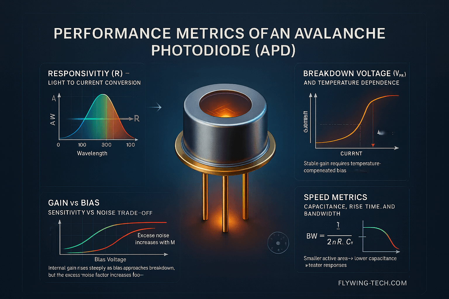
Responsivity (A/W)
Responsivity (indicated by $R$) tells how much the APD makes for a given light power, and its spectral curve shows which wavelengths it detects best.
Breakdown voltage ($V_{BR}$) & temperature coefficient
Breakdown voltage is the bias where avalanche becomes self-sustaining, and it moves with temperature, so stable gain requires temperature-compensated bias control around $V_{BR}$
Gain ($M$) vs bias; excess noise factor ($F(M)$)
The internal gain in APD rises steeply as bias approaches $V_{BR}$, but the excess-noise factor $F(M)$ also increases, trading higher sensitivity for degraded SNR.
Capacitance, rise time, bandwidth
The total input capacitance and avalanche build-up time set the $RC$ limits, so smaller area and higher electric field yield faster rise time and wider bandwidth, typically formulated as approximately $$BW=\frac{1}{2\pi R_{eq}C_T}$$ bound by the APD gain–bandwidth product.
| Parameter | Why It Matters | Typical Range |
|---|---|---|
| Responsivity | Converts optical input to current | 0.2–1 A/W |
| Gain vs Bias | Determines internal amplification | 10–200 |
| Excess Noise Factor F(M) | Lower is better for SNR | 1.5–4 |
| Capacitance | Limits bandwidth | few to 10 of pF |
| Rise Time / Bandwidth | Must support system data rates | 100s of MHz to 10s of GHz |
Avalanche Photodiode Use Cases
Telecom & Fiber Optics
In telecom optical communication, APDs boost receiver sensitivity and link reach in fiber networks by multiplying weak signals after fiber attenuation; they’re standard in 1310 nm and 1550 nm receivers. High-speed APDs with tens-of-GHz bandwidth enable 100-Gb/s links; for example, a 42-GHz APD has been demonstrated at low gain.
LiDAR, Rangefinding, and ToF Cameras
In laser-ranging and time-of-flight (ToF) systems, APDs pick up the light pulse that bounces back from a target, often in the 905 nm or 1550 nm range. Because the returned light is very weak, the detector must be very sensitive and react quickly to capture it. These needs shape the device design and the readout electronics.
Scientific & Medical Sensing
APDs read out scintillators, photoluminescence, spectroscopy, and photon correlation experiments in lab environments. They are preferred when PMTs are bulky or require high voltage in a compact system. In medical sensing, APDs help catch very weak, fast light signals often used in pulse oximeters, PET/CT detectors, and fluorescence tools. This is because the APD’s internal gain boosts sensitivity at low light levels.
Industrial & Safety Applications
In industrial and safety systems, APDs offer high sensitivity and rapid detection for low-light machine vision, thereby extending inspection capabilities to low-light environments on moving lines. Their internal gain and quick response improve barcode read range and speed under dust and dim lighting, while robust near-IR performance supports common scan wavelengths.
Avalanche Photodiode vs Photomultiplier Tube
When considering the selection between Avalanche photodiode vs photomultiplier tube (PMT), the following trade-offs are crucial to consider:
| Parameter | APD | PMT | Takeaway |
|---|---|---|---|
| Gain | ~10–200 (internal multiplication) | ~10^5 to 10^7 | PMTs deliver far higher gain for ultra-low light/photon counting. |
| Noise | (excess) noise & shot noise | Very low excess noise; sensitive to stray light | APDs trade some SNR for compactness; PMTs excel in faintest signals. |
| Size, power, durability | Solid-state, compact, rugged; low supply voltage | Vacuum tube; bulky; requires high voltage | APDs are easier to integrate and more robust. |
| Environmental resilience | Tolerant to magnetic fields, shock, vibration | Sensitive to magnetic fields; fragile | APDs suit harsh/industrial environments. |
| Typical use | Low to moderate light, fast & compact receivers | Extremely low light, photon counting | Use APDs for compact systems; use PMTs (or SPADs) when every photon counts. |
Testing, Characterization & Calibration
Reliable APD data requires repeatable methods and traceable calibration. If you often use APD or PMT devices in your project, you should also consider the quality assurance checklist at the end. For testing and calibration, define key parameters to report upfront, such as unity-gain responsivity $M(V)$, dark current at specified bias/temperature, rise time, and noise densities. Lock the calibration procedure to ensure consistency across different devices, days, and production lots.
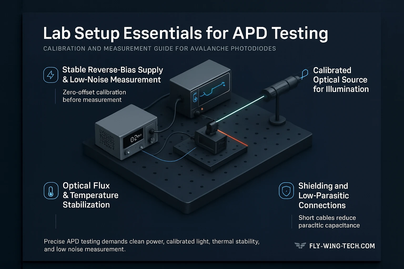
Lab Setup Essentials
- To begin the APD calibration, use a stable, low-ripple reverse-bias supply with fine resolution. Pair it with a picoammeter or low-noise current meter with guarded inputs and proper zeroing.
- Drive the APD with a calibrated optical source (laser or LED) verified against a traceable photodiode or power meter.
- Use neutral-density filters to control photon flux and a TEC stage to stabilize temperature.
- Minimize parasitics and stray reflections with proper shielding, or grounding, low-capacitance fixtures, short cables, and fiber conditioning.
Measuring Gain, Dark Current & Bandwidth
- Vary the voltage and measure how much current flows for different light levels to see how the gain changes with voltage.
- Find the baseline sensitivity without gain, then use it to calculate the actual gain at higher voltages.
- Measure the current in darkness at different voltages and temperatures to identify which leakage sources get amplified and which don’t.
- Send quick light pulses or modulated signals and capture the electrical output to measure response speed.
- Account for delays and distortions from your cables and measurement equipment before finalizing speed specifications.
- Use a dim light to prevent overloading the avalanche process, which can distort measurements.
Temperature Sweeps & Reliability Screens
- Test at different temperatures to see how breakdown voltage, sensitivity, and noise change, then create lookup tables to adjust bias voltage accordingly.
- Run burn-in cycles, temperature swings, humidity tests, and ESD checks to catch early defects and ensure stable long-term performance.
- Define safe operating limits and verify performance at extreme conditions (hot/cold, low/high voltage).
Quality Assurance Checklist
Keep a “golden” reference APD as a calibrated standard to benchmark each incoming lot. Periodically recalibrate this reference unit and use it to verify gain at target bias, dark current limits, bandwidth, and excess-noise factors for every new batch.
Establish a clear acceptance criterion and monitor results with statistical process control charts to catch deviations early and provide data-driven feedback to suppliers.
Maintain traceable records for each lot, including screening data, calibration dates, measurement uncertainty, and device genealogy to support audits and ensure long-term consistency.
Comparison of Photodetectors with APD
Choosing the right photodetector is about matching the required signal level, speed, and environment to the device’s strengths rather than matching a single specification. To effectively compare these devices, start by fixing the wavelength band and bandwidth, then compare SNR, gain mechanism, and biasing complexity. Let’s look at the top-level comparison of these in-category devices:
Avalanche Photodiodes vs PIN Photodiodes
A PIN photodiode has no internal gain. That is why it is simpler, has lower noise, and behaves linearly. Due to the absence of internal gain, it struggles when incident photons are scarce. In situations where photons are limited, APD shines and picks up weak signals effectively. However, with great power comes great responsibility to manage excess noise, tighter bias control, and compensate for temperature drifts.
If your link budget is tight or ToF timing is critical, APD gain can unlock a margin that a PIN diode cannot provide. When optical power is ample and you need wide bandwidth coverage and low distortion, a PIN diode with low noise is usually superior.
Avalanche Photodiode vs Photomultiplier Tube
An APD has a compact design, low-voltage operation, and it is easy to integrate on moving platforms, making it a strong choice for embedded receivers. On the other hand, a photomultiplier tube (PMT) wins for ultra-low light, and photon counting thanks to its exceptional (${10}^5$ to ${10}^7$) gain and off-the-chart low excess noise.
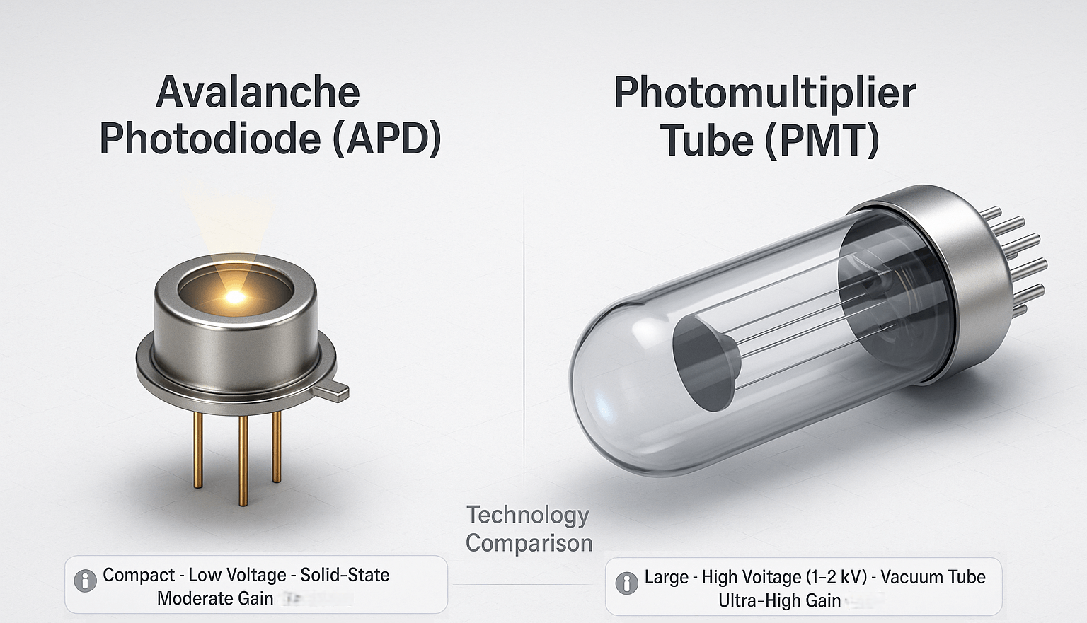
When the choice is between APD and PMT, pick APD for portable, space-limited, or harsh environments where high voltage and fragility are not suitable. Pick PMTs when every photon counts, the scene is extremely dark, and high voltage is acceptable.
Avalanche Photodiode vs SiPM
SiPMs (SPAD arrays) operate in Geiger mode, providing single-photon detection, precise timing, and digital outputs, but need quenching circuits, suffer from dark counts, afterpulsing, and pixel crosstalk, and saturate under bright light. APDs in linear mode give analog currents, simpler TIAs, and fewer saturation artifacts at moderate flux, with lower complexity in many fiber and industrial receivers.
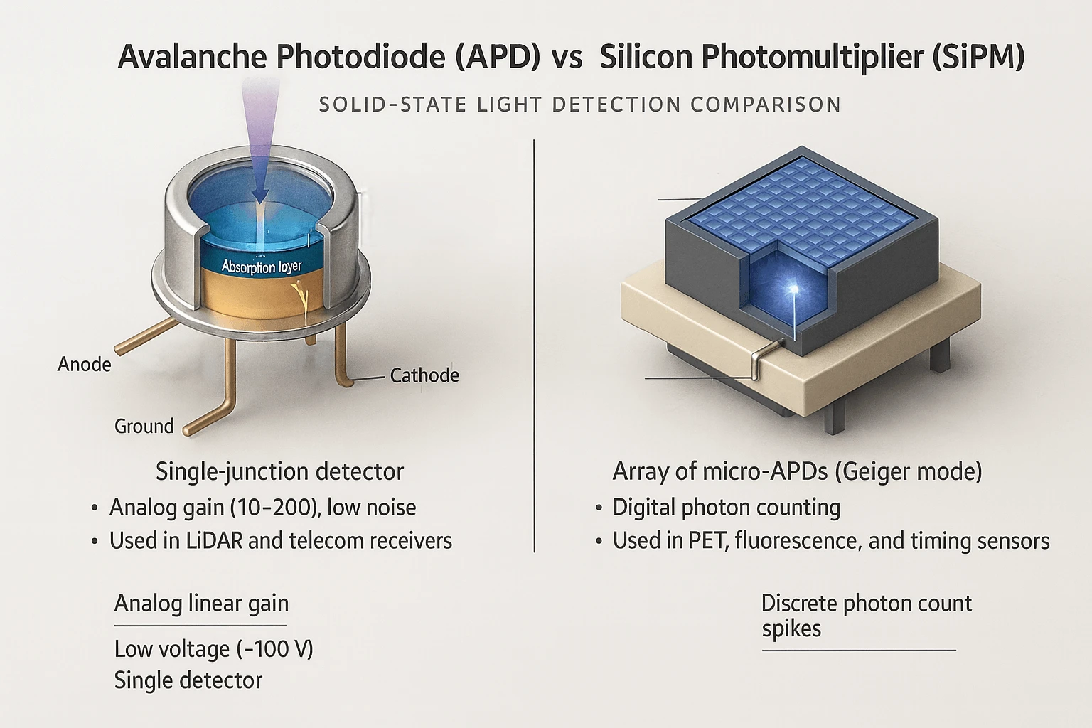
Choose SiPM for photon-counting, precise timing, or low-light imaging applications. Select APDs when you want analog linearity, moderate gain, and cleaner integration with conventional analog front ends.
Conclusion
An avalanche photodiode exploits controlled breakdown to amplify weak optical signals. This provides a high gain but increases noise. The key to using APD is biasing just below breakdown, where sensitivity peaks while excess noise stays manageable.
Understanding APD datasheets means examining linked parameters such as responsivity, gain versus bias, dark current, and bandwidth. Since each of these parameters reveals device behavior inthe circuit.
Properly matched to their application, APDs serve as versatile tools in telecommunications, LiDAR ranging, and scientific instrumentation, offering sensitivity, speed, and compactness essential for detecting light at its limits.
Glossary
| Terminology | Explanation |
|---|---|
| APD | An Avalanche Photodiode multiplies photocurrent internally via impact ionization. |
| PMT | A Photomultiplier Tube is a vacuum-tube detector that achieves high gain using dynodes to multiply electrons. |
| Impact Ionization | A high-energy carrier knocks another electron out of the lattice, creating an electron–hole pair. |
| Electron–hole Pair | A free electron in the conduction band and a hole left in the valence band after absorption. |
| Gain | The ratio of output current to primary photocurrent, often denoted $M$ |
| Photon | A quantum of light carrying energy $E=hν$ |
| Breakdown Voltage | The voltage at which the avalanche becomes self-sustaining. APDs operate just below this point. |
| Secondary Carrier | A newly created electron or hole is generated by impact ionization rather than by the original photon impact. |
| Absorption Region | The APD layer, where incoming photons are absorbed to generate primary carriers. |
| Multiplication Region | A high-field layer where carriers gain energy and trigger impact ionization. |
| LiDAR | Light Detection and Ranging measures distance by timing laser pulse returns. |
| InGaAs | Indium Gallium Arsenide is a compound semiconductor with strong sensitivity from ~900 to 1700 nm |
| InP | Indium Phosphide is a lattice-matched substrate and multiplication layer material for InGaAs APDs. |
| SAM Structure | Separate-Absorption-Multiplication stacks an absorber layer and a distinct multiplication layer. |
| Rise Time | The time to go from 10% to 90% of the final output after a step input. |
| SNR | The Signal-to-Noise Ratio compares the strength of the desired signal to the noise level. |
| Shot Noise | Random fluctuation from the discrete nature of charge and photon arrivals. |
| Geiger Mode | Operation above breakdown, where single photons can trigger a self-quenching avalanche. |
| SPAD | A Single-Photon Avalanche Diode is a Geiger-mode APD optimized for detecting individual photons. |
| SiPM | A silicon photomultiplier is an array of many SPAD microcells summed in parallel. |
| ToF Cameras | Time-of-Flight cameras measure distance by timing light travel per pixel. |
FAQs
An avalanche photodiode (APD) is a semiconductor light sensor that uses a high reverse bias to internally amplify signals. When photons hit, the impact ionization multiplies the carriers, creating a stronger current. This makes APDs ideal for low-light detection in LiDAR, optical communication, and medical imaging.
The avalanche effect starts when energetic electrons collide with atoms, releasing secondary carriers that multiply the signal. This internal gain boosts current without external amplification.
A PIN photodiode directly converts light to current, offering low noise without internal gain. An avalanche photodiode (APD) amplifies the signal internally, achieving higher sensitivity with increased noise.
An APD has an absorption layer and a high-field multiplication region, separated by guard rings. The avalanche region multiplies carriers under a strong electric field. This structure ensures stable performance and reliable gain control.
What determines the avalanche photodiode gain and noise performance?
APD gain increases with increased bias voltage, also raising the dark current and excess noise. The temperature, ionization ratio, and junction design also affect the APD gain performance.
A low-noise APD minimizes random gain variations, yielding a higher signal-to-noise ratio (SNR). This improved SNR allows the device to detect weaker optical signals more accurately in applications like fiber-optic communication, spectroscopy, and LiDAR sensing.
Three main factors influence the avalanche photodiode bandwidth and response time:
1. carrier transit time across the device layers 2. avalanche build-up time (which increases with gain) 3. external RC time constant (capacitance × resistance).
Properly regulated reverse bias controls the multiplication factor and prevents avalanche breakdown. Maintaining a stable bias voltage ensures a consistent APD gain and reduces temperature-induced drift.
Due to high-gain and sensitivity, APDs are used in LiDAR for high-resolution distance ranging, in fiber optics for high-sensitivity, high-speed optical receivers, and in medical sensing for PET scanners and pulse oximetry.
How does an avalanche photodiode vs a photomultiplier tube (PMT) compare in gain, cost, and ruggedness?
Compared to photomultiplier tubes (PMTs), APDs are solid-state, compact, and cost-effective, low-voltage devices with excellent reliability. Although PMTs offer higher gain, they are fragile and expensive.
When using a larger-area avalanche photodiode, it collects more photons, which makes it better at detecting weak or spread-out light. The downside is that bigger photodiodes have more capacitance, so a reduced bandwidth is achieved to get that improved light collection.
InGaAs APDs operate in the near-infrared range (900-1700 nm), ideal for telecom and LiDAR, while silicon APDs function in visible to near-IR (400-1000 nm). The material choice for APD defines wavelength range, noise, and gain performance.
In the selected APD product dataset, review responsivity, breakdown voltage, gain, capacitance, and bandwidth. These parameters determine circuit design choices for noise, speed, and temperature compensation.
For a high-bandwidth, low-noise APD circuit, use a clean, temperature-compensated bias voltage supply and a low-noise transimpedance amplifier (TIA). Also, short PCB traces and shielding help achieve high-bandwidth, low-noise APD circuit design.
Typically, APD prices vary based on the active area, material (Si or InGaAs), and screening grade. Buyers can find cost-effective APD photodetectors from trusted suppliers like Fly-Wing Tech.