Introduction
MOSFETs stand for Metal Oxide Semiconductor Field Effect Transistors. These transistors are voltage-controlled devices, which means their conductivity is determined by the voltage applied at the gate terminal, known as Vgs (gate to source voltage). The MOSFET transistors come as a three-terminal device known as Gate, Source, and Drain.
In many electronics applications, such as half-bridge and full-bridge inverters, there is a need to simultaneously drive low-side and high-side MOSFET transistors. In such situations, MOSFET drivers are used, and one such popular driver is the IR2110 MOSFET Driver. The IR2110 MOSFET drivers are specialize circuits because they are capable of controlling the gate voltage of both low-side and high-side transistors simultaneously and making the MOSFETs switch ON and OFF quickly. Due to the IR2110 driver’s capability of controlling high voltage and high power MOSFETs, IR2110 MOSFET drivers are widely use in various applications, including motor drive circuits, switch-mode power supplies, and inverter circuits.
IR2110 as MOSFET Driver
The IR211O MOSFET driver ICs are high-voltage, high-power driver circuits that are widely use in half and full bridge circuits to drive both high and low side switches. These drivers consist of independent low-side and high-side reference output channels. The operating voltage range of IR2110 is between 10-20 volts with an output current of 2.0 Amps. Generally, the IR2110 driver comes in 16-PIN SOIC and 14-PIN PDIP packages. It also consists of a specialize channel design to handle high-side transistor output using a bootstrap operation.
The bootstrap operation is essential because, on the high side, we connect the source terminal of the MOSFET with the load as shown. Therefore, to turn it ON, it generally requires a higher voltage compare to the low-side output transistor. To provide the higher voltage, we use a bootstrap capacitor, which is discuss later in this article.

As a design engineer, you must be aware of some of the core parameters of IR2110 to better utilize it in a circuit, as listed in the Table. For all technical and parameters, please refer the official datasheet of IR2110 motor drive IC.
IR2110 MOSFET Driver IC Core Parameters
| Parameter | Value | Core Function |
|---|---|---|
| Low-side Supply Voltage (VCC) | 10–20 V | Provides gate drive voltage to the low-side MOSFET |
| High-side Supply Voltage (Vs) | Above 20 V | Provides gate voltage to the high-side MOSFET |
| Output Gate Current (HO/LO) | 2.0 A | Quickly charges/discharges the MOSFET gate capacitance |
| Logic Input Voltage (LIN/HIN) | 3.3 V / 5 V | Interfaces with microcontrollers and logic ICs |
| Operating Temperature | –40 °C to +125 °C | Enables IR2110 use in industrial and automotive applications |
IR2110 MOSFET Driver PIN Configuration
The IR2110 drivers are mostly comes in two packages, i.e., 16 PIN SOIC and 14 PIN PDIP. However, the SOIC package is more popular and used in a wide range of power electronic applications, especially in power conversion and motor drive.
| PIN Configuration of IR2110 MOSFET Driver | ||
|---|---|---|
| PIN Number | PIN Name | PIN Function |
| 1 | LO | Low-side MOSFET output. |
| 2 | COM | This PIN is the GND of the low-side supply. |
| 3 | VCC | Low-side supply (10–20 V). |
| 6 | VS | High-side floating supply return. |
| 7 | VB | High-side MOSFET floating supply voltage. |
| 8 | HO | High-side MOSFET output. |
| 11 | VDD | Logic supply (3–20 V, typically 5 V). Logic 1 = +5 V, Logic 0 = 0 V. |
| 12 | HIN | High-side MOSFET logic input. |
| 13 | SD | Shutdown PIN. Low = Enabled, High = Outputs OFF. |
| 14 | LIN | Low-side MOSFET logic input. |
| 15 | VSS | Logic supply GND. |
Note: PINS 4,5,9,10,16 are Not Connected (NC).
IR2110 Circuit Design
IR2110 MOSFET drivers are widely used in power electronic applications, such as half-bridge, full-bridge circuits, switch-mode power supplies, and inverter circuits. This section explains the half-bridge circuit design with the IR2110.
A half bridge consists of a high-side and low-side MOSFET. The IR2110 MOSFET driver needs to be configure before it can drive both MOSFETs effectively. The +VCC PIN is a low-side supply, and according to its datasheet, it must be connected to a 10–20 Volt supply. The VDD PIN is a logic supply input, and it must be connected with a +3V to +20V power supply. However, the VSS is the return of the logic supply, and COM is the return of the low-side supply and therefore must be connected with GND.

Figure 1: IR2110 Driver circuit with high side and low side MOSFET
HIN and LIN are the logic inputs to IR2110. so, when we apply a high signal (Logic 1) at the HIN input, it drives the HO output, resulting in high-side (Q1) MOSFET ON. Similarly, when we apply a high signal (Logic 1) at the LIN input, it drives the LO output, resulting in low-side MOSFET (Q2) ON. However, the source terminal of the low-side MOSFET is directly connected to GND. Whereas, the source terminal of the high-side MOSFET is connected with the floating supply return (VS).
In the next section, I will explain how a bootstrap capacitor is use for a floating supply and drive the high-side MOSFET. The VCC, VS, and VB PINs are use for this purpose. SD pin is the shutdown PIN and when we connect the SD PIN with GND, the IR2110 is functional. However, keeping this PIN high makes the IR2110 disable, which means all the outputs are turn OFF.
Bootstrapping in IR2110
In a half H-bridge circuit, we do not connect the source terminal of the high-side MOSFET is to the GND, but rather we connect it to the floating supply, as shown in Figure 1. In such situations, the bootstrap capacitor is use to make the floating supply a few volts higher than the source terminal.
When the low-side MOSFET is ON, the bootstrap capacitor is charge through the diode. When the high-side MOSFET turns ON, the IR2110 makes the HO output high with respect to VS. This is done using the stored charge from the bootstrap capacitor to raise the gate voltage above the source. A common rule to calculate the bootstrap capacitor is to use the following formula.
\[
C_{\text{boot}} \geq \frac{Q_{g} \times N}{\Delta V}
\]
Where Qg is the MOSFET gate charge, and is the allowable voltage drop. Cboot is the bootstrap capacitor, and N is the number of switching events before the bootstrap capacitor is refresh. The number of switching events always refers to the high-side MOSFET. Usually, in PWM operation, the N is often taken as 1 because the capacitor charges each time when the low-side MOSFET turns ON. The value of Qg is easily found in the datasheet and is usually in nC.
Typical values of the bootstrap capacitor are between 100nF to 1uF. The positive terminal of the capacitor is connected to the VB, and the VS PIN (floating supply return) is connected to the negative terminal of the capacitor and the source terminal of the high-side MOSFET.
When LIN=1, HIN=0:
When the LIN is high (Logic 1), the Q2 MOSFET is ON. During this time, the capacitors C1 and C2 are charge up to the level of VB.
When LIN=0, HIN=1:
The bootstrap capacitor that is charge up to the level of VB during the MOSFET Q2 ON duration is now use to add extra voltage above the source level to drive the high-side MOSFET. For comprehemsive theoratical concepts of motor drive circuits refer the offical “Application Report” on MOSFET and IGBT gate driver circuits.
Resistor Selection for IR2110
Generally, 5–20-ohm resistor values are use at the gate terminal of MOSFETs to reduce the oscillations and balance the switching speed. A gate to source pull-down resistors is use to keep the MOSFET in the OFF condition when the output is floating and to prevent the MOSFET from any false ON condition.
| IR2110 Resistor Values Selection | ||
|---|---|---|
| Placement of Resistors | Typical Values | Function |
| Gate resistors | 5 to 20 Ω | To reduce oscillations |
| Gate-source resistors | 1k–10k | To prevent a false ON condition |
Common Circuit Applications with IR2110
IR2110 MOSFET drivers are high-power drivers that are extensively use in power electronic applications, including DC-DC converters, H-bridge circuits to drive DC motors. In this section, I will explain a couple of applications with IR2110 MOSFET drivers.
-
H-Bridge to drive the DC Motors

DC motors are one of the most widely use electronic component, and to drive the DC motor, a simple circuit is use, known as the H-bridge circuit. The H-bridge circuit is made using two identical half-bridge circuits shown in the figure above. Only two N-channel MOSFETs and one IR2110 driver are use to made a half bridge circuit. However, four N-MOSFETs and two IR2110 drivers are use to made the H bridge circuit. This is important because to drive the motor in both forward and reverse directions, we need two half-bridges. The half-bridge circuit is use to drive the motor in either the forward or reverse direction. However, when two half bridges are use in combination, it can drive the motor in both forward and reverse directions.
Q1= 1 (Logic High), Q4=1 (Logic High) & Q3=0 (Logic Low), Q2=0 (Logic Low)
When the Q1 and Q4 are at logic high and the remaining two MOSFETs are at low logic, the current will flow from the positive terminal of the motor to the negative terminal of the motor, and it will move the motor in the forward direction.
Q2= 1 (Logic High), Q3=1 (Logic High) & Q1=0 (Logic Low), Q4=0 (Logic Low)
When the Q2 and Q3 are at logic high and the remaining two MOSFETs are at low logic, the current will flow from the negative terminal of the motor to the positive terminal of the motor, and it will move the motor in the reverse direction.
Dead Time in H bridge Circuit
Another important design parameter that must be consider in the design is the dead time to prevent the MOSFET from destruction. Sometimes, a condition occurs when both the low-side and high-side MOSFETs turn ON simultaneously, creating a short circuit condition. To prevent such a condition from occurring, dead time is introduce between the ON/OFF times of low low-side and high-side MOSFETs.
Dead time is introduce in the logic circuit or in the microcontroller programming environment that generates the HIN and LIN signals. Typically, dead time is set between 200ns to 1us.
2. Speed Control of Fan using IR2110

Another example of IR2110 is fan speed control. IR2110 is use to drive a single MOSFET using the bootstrap circuit. We connect the MOSFET drain terminal with the +VCC and source terminal with the postive terminal of fan. We connect the negative terminal of the fan with the GND as shown in figure above. The microcontroller generates the PWM signals that are fed to the HIN and LIN of IR2110. Using the PWM, the IR2110 turns ON/OFF the MOSFET. By adjusting the PWM signal, the average voltage across the fan is changing, which results in the speed control of the motor.
How to Use IR2110 in Your Circuit
Appropriately using the IR2110 in your circuit application requires careful attention and a step-by-step approach.
-
IR2110 Configuration
Properly configure the IR2110 driver IC according to the specific application. Make sure to connect the VCC and VDD with the correct voltage as discussed earlier in the article (refer to the datasheet). Make sure to place the capacitor close to the VCC and VDD pins.
-
Logic Inputs
Ensure to precisely generate the HIN and LIN logic inputs of IR2110. The 555 timer IC and microcontrollers are a good choice for generating these inputs.
-
Bootstrap capacitor
If your application is using IR2110 to drive the high-side MOSFET, make sure to accurately calculate the bootstrap capacitor as discussed earlier in this article.
-
Output Connections
Connect the HO with the high-side MOSFET and connect the LO with the low-side MOSFET for proper operation of the circuit. Refer MOSFET driver datasheet for HO, LO PINS. The IR2110 has PIN 7 as HO and PIN 1 as LO.
Simulation Results: Buck Converter Using IR2112
In this section, I have simulated the buck converter circuit design using the MOSFET Driver IR2112. A buck converter is a step-down converter that takes the DC input voltage and steps down the voltage. The output of the buck converter is determine using the duty cycle. The duty cycle ‘D’ of the buck converter is find out using the formula.
\[
D = \frac{V_{\text{out}}}{V_{\text{in}}}
\]
Where Vout is the buck converter output voltage, and Vin is the maximum input voltage.
The microcontroller generated the PWM that is fed into the HIN PIN of the IR2112 IC. The IR2112 generates the high pulse at the HO PIN, and it drives the MOSFET IRF470. By using the PWM signal, the average voltage is step down at the output of the buck converter.

Buck Converter circuit with MOSFET Driver

PWM Generation from the Microcontroller
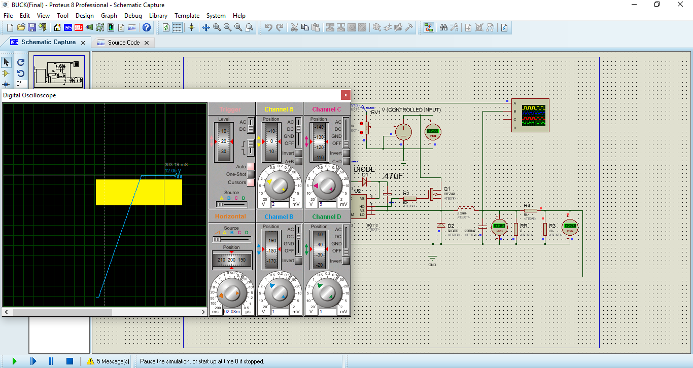
Output Waveform of Buck Converter
In the simulation section, I have used the IR2112 driver IC because it is easily available in the simulation software. Both IR2110 and IR2112 share the same functionality of driving the low-side and high-side MOSFETs. However, IR2112 has a built-in feature of a dead-time logic function.
Conclusion
In conclusion, the IR2110 MOSFET driver IC is a powerful driver that is widely use in power electronic applications, including H-bridge circuits, DC-DC converters, and many more. Therefore, It is important for the electronic design engineers to understand the fundamentals of the IR2110 IC to better use it in their circuit designs. Understanding IR2110 driver PIN Configuration, Bootstrapping, and resistor selection is important for engineers to design and innovate electronic applications.
Frequently Asked Questions (FAQ)
Q. Why is Bootstrap Capacitor use in the IR2110 Circuit?
Bootstrap is use to drive the high-side MOSFET. The bootstrap capacitor that is charge up to the level of VB during the MOSFET Q2 ON duration is use to add extra voltage above the source level to drive the high-side MOSFET.
Q. Is it important to connect the SD PIN with GND?
Connect the SD PIN with GND. If not, the IR2110 may misbehave or not work properly.
Q. What is the typical value of Bootstrap Capacitor?
The typical value of the bootstrap capacitor is between 100nF to 1uF.
Q. What is the referenced Return of High-side MOSFET in IR2110?
The return of the high-side MOSFET is VS (PIN 5) of IR2110.