Introduction to 74HC595 Shift Register IC
The 74HC595 shift register is an 8-bit CMOS integrated circuit that uses serial-to-parallel conversion. It is usually used to increase the number of output pins on microcontrollers such as Arduinos and allows microcontrollers to control an additional 8 digital outputs (and more when using multiple devices) with only 3 signal lines (serial data in, shift clock, and latch clock).
74HC595‘s limited ability to use GPIO (General Purpose Input/Output) pins makes them extremely useful in applications where GPIO pin resources may be limited. Common applications include driving LED arrays, 7 segment displays, relay modules, and indicator lamps in embedded systems. The 74HC595 is an integrated circuit in the HC (High-Speed CMOS) family of logic devices and offers low quiescent current and a wide supply voltage range (3.3V-5.0V) and is compatible with 3.3V and 5.0V logic levels if the input voltages are of the appropriate threshold level.

The internal parts of the 74HC595 Shift Register include Two Key 8 Bit Registers:
- Shift Register (SR) – Receives serial data input one bit at a time with every rising edge of the shift clock (SRCLK/SHCP) .
- Data Register (DR) – The transfer of the contents of the shift register (SR) to the parallel output pins (QA-QH) occurs at the rising edge of the latch clock (RCLK/STCP) .
Having separate shift and data registers keeps new data flowing into the shift register without interfering with existing output until the data register is latched. This allows for smooth transitions between consecutive outputs in applications that use multiplexing or require precise timing.
Key advantages in practice:
- The pin count on the microcontroller is minimized from over eight down to three pins (data, clock, latch).
- Supports daisy chain connections for virtually unlimited output expansion.
- Tri-state outputs (/OE controlled) allow for bus sharing and power-down modes.
For accurate electrical data, check manufacturer-supplied manufacturers (for example, the current revision of SN74HC595 or other NXP or ON Semiconductor devices), since there are slight differences between manufacturers.
Key Specifications and Datasheet References
Important note on current limits:
Individually, the pins of the 74HC595 can manage a current of approximately 20-35mA for LEDs with the corresponding current-limiting resistors of 220-330 ohms connected to 5 volts. However, the overall sink/source current through the device must be kept below the absolute maximum limitation of the package (usually 70mA continuous at 25 degrees C). Exceeding the maximum limit may result in the item going into thermal shutdown, having lower voltage output, and possible permanent damage to the device. Always remember to calculate out the total load when using multiple LEDs or relays to drive the 74HC595.
Due to these specifications of the 74HC595 shift register, they make for a great choice for the majority of hobbyists and semi-professional Arduino projects, but when you want to operate relay coils or motors with higher current draw you may want to consider using alternative devices that can supply more current such as: the TPIC6B595 (open drain, 150mA per channel) or the ULN2803 Darlington array type devices.
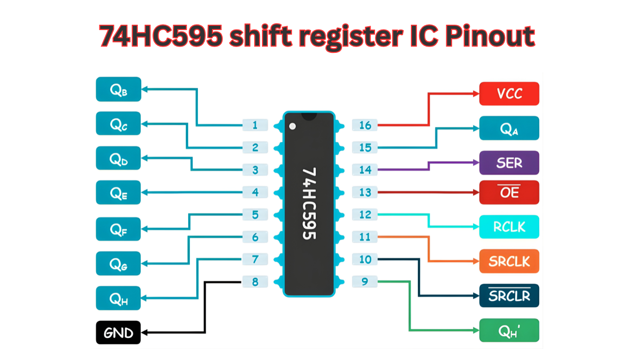
74HC595 Pinout and Configuration
The 74HC595 shift register uses a standard 16-pin DIP, SOIC, or TSSOP package. Correct pin identification and function understanding are essential to avoid common wiring errors that cause no output, random flickering, or data corruption.
Below is the complete pinout (viewed from the top, notch or dot on the left):
Practical wiring notes:
- Pin 8 and VCC will always connect to Pin 16 pins to verify that both are on the same board and to ensure that both pins are receiving power as well as ground. A 0. 1 microfarad ceramic decoupling capacitor should also be placed between these two pins so that any noise will not cause a glitch in operation from power or ground to the input.
- The /OE (an output enable) pin does need to be connected to ground on this device to operate normally; any connection of the /OE pin to anything that is not a ground could produce undefined results from this device’s output.
- The /SRCLR pin is not needed for regular operation, but if you short that pin to supply voltage and then send a “low” pulse to that pin, it will clear the shift register.
- Lastly, the Q7S pin will be used to connect to the serial data output (pin 9) of the last device in a cascade (to connect to the serial data input of the next device in a cascade).
Pin Functionality Breakdown
Input and Clock Pins
- SER/DS (PIN 14): Serial data input. Samples receive data on the rising edge of SRCLK. Send bits in either MSB (most significant bit) first or in LSB (least significant bit) first order depending on what you specify with your shiftOut() command. (Default in Arduino is MSBFIRST)
- SRCLK/SHCP (PIN 11): Shift clock. Each rising edge of SRCLK shifts the current 8-bit register one position to the right (with the oldest bit becoming the bit shifted out to Q7S) and with the new data received from DS being entered into the least significant bit position.
- RCLK/STCP (PIN 12): Latch or storage clock. Each rising edge transfers all of the data contained within the shift register in one clock cycle to the storage register, thereby updating all Q0-Q7 outputs simultaneously (and preventing any transient ‘glitching’ from occurring during the shifting process).
Control Pins
- /OE (pin 13): Output Enable / Active Low / Will drive outputs Q0 – Q7 normally when Low (GND); will drive outputs Q0 – Q7 High Impedance (Tri-State) when High (VCC or Floating with Pull-up). Useful for Multiplexing or Power Savings.
- /SRCLR/MR (pin 10): Master Reset / Active Low / Any Low Pulse will clear the Shift Register Asynchronously (All bits set to 0); the Storage Register will remain unaffected / require the Latch to clear outputs after the reset.
Output Pins
- Q0–Q7 (pins 15,1–7): Parallel outputs (QA to QH in some datasheets). Q0 is LSB, Q7 is MSB.
- Q7S (pin 9): Serial output from the last stage. Used for cascading (connect to next DS) or monitoring shifted data.
Features of 74HC595 Shift Register
The primary features of the 74HC595-based shift register are sufficient to provide numerous GPIOs (general-purpose input/output pins) in your microcontroller based design. The shift register is an 8-bit device, having a secondary 8-bit storage/latch register and tri-state outputs. These three operations allow for fast and glitch-free conversion of the serial input data into parallel output data when it’s transferred to the output buffers of the register.
Key structural features include:
- The 8-bit Serial-in, Parallel-out device has independent shift and storage registers. Data is received into the device through the Serial Data Input (DS) pin. The data is shifted out of the register on each rising edge of the Shift Clock (SRCLK). When data is shifted out, it goes into the Storage Register on the rising edge of the Register Clock (RCLK) which provides all eight parallel outputs (Q0 – Q7) simultaneously.
- Tri-state outputs controlled by the active-low /OE pin. When /OE is low, outputs actively drive high or low; when high, outputs enter high-impedance state, allowing multiple devices to share a common bus or enabling power-down modes.
- Cascadable design via the Q7S (serial output) pin, which provides the shifted-out bit from the last stage. Connecting Q7S of one IC to SER (DS) of the next allows expansion to 16, 24, or more bits with shared clock and latch lines.
- An asynchronous master reset (/SRCLR or MR, active-low) is provided to reset the shift register contents regardless of the clock signal; therefore, the Storage Register is not cleared until a register latch pulse has been received.
- High-speed CMOS (HC) technology offering low static power dissipation, good noise immunity, and compatibility with TTL input levels at 5 V supply.
These features support reliable operation in applications requiring stable, glitch-free output updates, such as LED multiplexing or relay control.
Advanced Features and Limitations
- Speed and timing : Max clock frequency (100 MHz, Typical), 5V, 25°C. Practical limits for “hobbyist” setups (breadboards / long wires) are usually between 5-20 MHz due to signal integrity issues. Propagation delay (SRCLK to Q7S) is typically 13-20 ns.
- Output characteristics: Each output can source or sink up to ±6 mA continuously at 4.5–5.5 V (with voltage drop considerations); short-term peak currents approach ±35 mA per pin. Total package current is limited (typically 70 mA continuous at 25 °C for plastic DIP, derate with temperature). Always use current-limiting resistors (e.g., 220–330 Ω for LEDs at 5 V) to stay within safe bounds.
- Power and ESD protection: Quiescent current (low), <80 µA max @ 6V. Built in ESD protection (human body model ~2 kV) and latch-up immunity enhances reliable real life handling.
- Wide voltage range: Fully functional from 2.0 V to 6.0 V, with logic thresholds shifting accordingly (e.g., at 3.3 V, VIH min ≈ 2.31 V, suitable for direct 3.3 V microcontroller interfacing without level shifters in many cases).
Limitations to consider in design:
- There is no current drive available to handle large current drain (greater than 20 mA) products such as relays => you will need an external driver; either a ULN2803 or a TPIC6B595 with an open-drain 150-mA sink will work.
- Without proper decoupling (i.e. 0.1-µF ceramic with an optional 10-100 µF electrolytic capacitor across VCC to GND), the outputs can be susceptible to power rail noise.
- The outputs can also exhibit shoot-through or excessive current draw if the loads exceed the ratings or if they are shorted.
- There is no automatic power-on reset of the outputs when powered up (the output can be in an indeterminate state); you will have to either tie the /SRCLR pin to ground for a brief period of time at power-up or initialize the TT6887 via software.
Arduino Interfacing with 74HC595 Shift Register
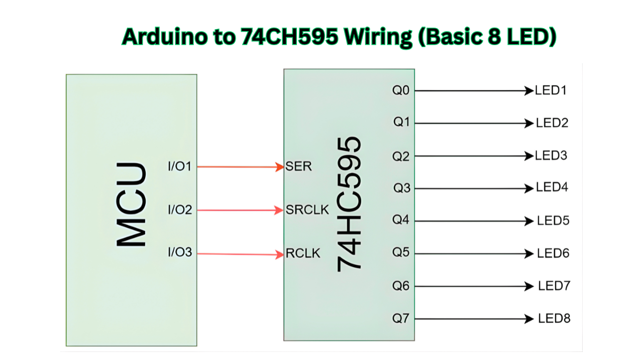
Using an Arduino with a 74HC595 shift register will allow you to expand the number of digital outputs from your device far beyond what is available with just the hardware pins of the microcontroller. There are only 3 signal lines needed for the connection along with power and ground, as a result this method is also efficient in controlling devices such as LEDs, relays, 7-segment displays and any device capable of loading bits in parallel.
Basic Hardware Setup (Single 74HC595)
Standard recommended pin mapping for Arduino Uno, Nano, or Mega (5 V logic):
Important electrical notes:
- The 74HC595 can be used reliably when powered at a supply voltage of 5V. When directly interfacing with 3.3V Arduino boards (like the Due, Zero and MKR series), the 74HC595 can be used because the input of the HC family of ICs will accept a logic level of 3.3V (where VIH minimum is about 2.31V at VCC of 3.3V). However, this also means that the high level output will be approximately 3.3V.
- The total package current should be limited to a maximum of approximately 70mA continuous at 25°C. For example, when using 8 LEDs in the output of the 74HC595 at 10-15mA each, the total current draw could approach this limit; so higher value resistors should be used to limit current or fewer LEDs should be used simultaneously at the output of the 74HC595.
Basic Circuit Schematic Description
The circuit is minimal:
- Arduino supplies power and three control signals.
- Outputs Q0–Q7 drive LEDs (or other loads) through current-limiting resistors.
- No pull-up or pull-down resistors are required on control lines when using short connections (<30 cm) and clean breadboard/power layout.
Common beginner mistakes to avoid:
- Forgetting the decoupling capacitor → causes random flickering or corruption.
- Leaving /OE floating → outputs may be tri-stated (no drive).
- Connecting SRCLK and RCLK to the same pin → data shifts but never latches to outputs.
- Reversing VCC and GND → destroys the IC instantly.
This basic setup forms the foundation for all 74HC595 projects with Arduino. The next subsections cover software implementation using both the classic shiftOut() method and the faster hardware SPI approach.
Advanced: Hardware SPI Interfacing with 74HC595
The use of hardware SPI to control a 74HC595 shift register is much more efficient than using the software-based, bit-banging because the Arduino’s built-in SPI peripheral transfers bytes using the hardware, which will result in approximately a 10x – 20x speed increase in transmission over bit-banging (depending on the clock divider configuration) and greatly reduced CPU overhead. This can be important and noticeable when:
- Updating high-frequency LED matrices or POV displays.
- Driving four or more cascaded shift registers (longer shift sequences).
- Running time-sensitive loops with other tasks (sensor polling, interrupts, etc.)
The 74HC595 has the same characteristics as SPI mode 0 (CPOL=0, CPHA=0), sampled on the rising clock edge and the clock idles low; just like the behavior of the shift register’s SRCLK(HC293) output.
Note: The SS pin (10 on Uno) is not automatically used for latching — you must control the latch pin manually with digitalWrite() before and after SPI.transfer() calls.
Key Implementation Notes
- Initialize with SPI.begin(), SPI.setBitOrder(MSBFIRST), SPI.setDataMode(SPI_MODE0).
- Optional: SPI.setClockDivider(SPI_CLOCK_DIV2) for ~8 MHz on a 16 MHz Uno (safe and fast; 74HC595 supports up to ~100 MHz theoretically, but keep <20 MHz in practice for clean signals).
- For single register: One SPI.transfer(byte) call per update.
- Latch sequence: Pull latch low → transfer byte(s) → pull latch high (rising edge latches data).
Cascading Multiple 74HC595 Shift Registers
To expand beyond 8 outputs, daisy-chain multiple 74HC595 ICs. The serial output Q7S (pin 9) of one IC connects directly to the serial input SER/DS (pin 14) of the next. Shared clock (SRCLK/SHCP) and latch (RCLK/STCP) lines control all registers simultaneously.
Daisy-Chain Wiring
- First IC: As in single-IC setup (SER from Arduino or previous Q7S)
- Subsequent ICs: Pin 9 (Q7S) of previous → Pin 14 (SER/DS) of next
- All ICs share: Pin 11 (SRCLK), Pin 12 (RCLK), Pin 13 (/OE to GND), Pin 10 (/SRCLR to VCC), VCC/GND
- Add 0.1 µF decoupling per IC, close to each package
- For hardware SPI: Same shared SCK/SCK and manual latch; send bytes in reverse order (last register first)
Multi-Byte Shifting
- With shiftOut(): Call shiftOut() multiple times (once per register) before one latch pulse. Send data for the farthest register first (due to shift direction).
- With hardware SPI: Call SPI.transfer() multiple times in sequence (e.g., SPI.transfer(highByte); SPI.transfer(lowByte);), then latch high. Again, send last register’s byte first.
Timing Considerations for Longer Chains
- Longer chains increase total shift time → use hardware SPI for better performance.
- Ensure clock pulse width meets datasheet min (typically >20 ns high/low at 5 V).
- Signal integrity: Keep wires short (<30 cm total), use ground planes or twisted pairs for clock/data if noise appears (random bits or flickering).
- Power supply: Longer chains draw more current → add bulk capacitance (10–100 µF) near the chain; monitor total draw against ~70 mA package limit per IC.
- Test incrementally: Start with 2 ICs, verify all outputs update correctly before adding more.
Troubleshooting 74HC595 with Arduino
When you write correct code for an application that uses the 74HC595 shift register and wire everything up correctly, you will sometimes still see unpredictable results because of one of three things: hardware issues, signal integrity, or failing to apply the correct control pin states. Below is a list of the most common issues related to the 74HC595 reported in various Arduino forums (and other; see the Resources section below), as well as some methods of systematically diagnosing the problems and suggestions for fixing them.

No Outputs / All LEDs Off
- /OE (pin 13) not grounded: If /OE is floating or high, outputs are tri-stated (high-impedance) — no drive capability. Fix: Tie pin 13 directly to GND. Many tutorials omit this; always verify.
- /SRCLR (pin 10) not pulled high: If low or floating, shift register stays cleared. Fix: Connect to VCC (5V). For reset capability, add a pull-up resistor (10kΩ) and optional momentary switch to GND.
- Power issues: Reversed VCC/GND or no power to pin 16/8. Fix: Double-check polarity; measure ~5V between pins 16 and 8 with multimeter.
Random / Flickering / Ghosting LEDs
- Missing or poorly placed decoupling capacitor: Latch transitions or power rail noise from switching will produce glitches when an LED chain goes from on to off or vice versa. To eliminate these glitches, add a 0.1 µF ceramic capacitor across pins 16 (VCC) and 8 (GND), leading to the shortest possible leads (ideally soldered directly under the IC on a perfboard). If there is a long LED chain or high current, add a 10 to 100 µF electrolytic capacitor near the LED chain.
- Loose breadboard connections or stretched contacts: Intermittent contact causes flickering when pressing wires. Fix: Reposition IC/wires to fresh breadboard area; test continuity with multimeter; consider soldering for reliability.
- Signal crosstalk / long wires: Clock (SRCLK) and latch (RCLK) lines pick up noise if parallel without ground separation. Fix: Shorten wires (<30 cm total), route clock lines away from each other, add ground wires between signals if using ribbon cable.
Data Corruption / Only First Few Outputs Work (Especially in Chains)
- Incorrect bit order or latch timing: The data will shift through timelining; if it is not latched then it will not send signals properly to the next device. To fix this issue, ensure that you are using MSBFIRST (the default for shiftOut) and that you are latching the data after all of the bytes have been shifted out. In addition, for SPI prototyping, make sure the device is programmed to automatically latch when using Mode 0.
- Noise on clock/latch lines: When there are long daisy chains, you may miss timing edges due to poor signal quality. Some options to improve the signal quality are to slow down the clock by adding a small delay between the bits, use level shifters (for the 3.3v Arduino), and put 100-1000 ohm resistors in series with the clock signal to provide some damping.
- Cascading wiring error: Q7S not connected to next DS, or shared clocks missing. Fix: Verify daisy-chain; send bytes in reverse order (farthest register first).
All LEDs Always On / Stuck Outputs
- Power-up state indeterminate: Outputs may power up random/high without initialization. Fix: Pulse /SRCLR low briefly on startup (or tie low then high); send known data (e.g., 0x00) in setup().
- Excessive current draw / voltage drop: Too many LEDs at high current → brown-out or damage. Fix: Use ≥220 Ω resistors per LED; limit simultaneous on LEDs; measure supply voltage under load.
Intermittent Behavior or Arduino Resets
- Current overload or separate supplies without common ground: Voltage drops or floating ground due to resets/randomness. Solution is to have a good common GND between Arduino & Shift register circuit and ideally run them off the same power source.
- Floating inputs during power-up: Noise clocks in garbage data. Fix: Add pull-down resistors (10kΩ) on SRCLK/RCLK if needed (rare); initialize in code.
3.3V Arduino Compatibility Issues
- Logic level mismatch: Some HC inputs need higher VIH at lower VCC. Fix: Direct connect usually works at 3.3V VCC (thresholds shift), but test; use HCT version or level shifter if unreliable.
Debugging Tools and Steps
- Measure voltages: VCC=5V, /OE=0V, /SRCLR=5V.
- Test with simple code: Shift 0xAA (alternating pattern) and observe.
- Use multimeter/LED tester on outputs directly.
- Oscilloscope (if available): Check clean rising edges on SRCLK/RCLK, no ringing.
FAQ – 74HC595 Shift Register
Data enters the register each time there is a rising edge on the SRCLK signal. The data entered into the register will stay latched, to the outputs, during the rising edge of the RCLK signal.
Use 0.1µF ceramic capacitors to filter the noise on your power supply that may distort your shifting timing and cause flicker. Place these 0.1µF capacitors as close to the VCC(pin 16) and GND(pin 8) connection points as possible.
Yes, but limit to ~6–20 mA per pin with 220–330 Ω resistors at 5 V. Total package current should stay below ~70 mA continuous to avoid damage.
Pulse /SRCLR (pin 10) low briefly (asynchronous clear of shift register), then latch with RCLK to update outputs. Tie it high for normal use.
Usually caused by missing decoupling, excessive current draw, or incorrect wiring (e.g., swapped VCC/GND). Add capacitors and verify connections.
Yes, supply range is 2–6 V and logic thresholds adjust. Outputs swing to 3.3 V; most downstream devices accept it, but test for reliability.
Practical Applications of 74HC595
The 74HC595 shift register is frequently used when a microcontroller needs to control more digital outputs than available GPIO pins allow. Its low pin count (3 signals + power/ground) and cascading capability make it ideal for several classes of projects.
- Driving LED matrices and bar graphs Several cascaded integrated circuits (ICs) like the 74HC595 chip control either the columns or rows of an LED matrix (i.e., an LED display measuring 8×8 or larger) for scrolling text, animations, or simple graphic images. When you latch the output, it provides a stable column/row selection for scrolling all of the displayed elements.
- Controlling 7-segment displays One 74HC595 can drive one common cathode or common anode 7-segment digit (including a decimal point) on its 8 outputs. By cascading additional 74HC595 shift register chips together, you can make multiple digits without taking up a lot of Arduino pins.
- Relay and solenoid arrays With the right supporting components (ULN2803 Darlington Array, discrete transistors), the 74HC595 can be used for controlling a bank of relays, solenoids, or opto-isolators for home automation, industrial control, or test equipment.
- GPIO expansion in IoT sensor nodes and robotics The 74HC595 also works great with battery powered IoT devices and robot controllers. It provides additional outputs for status LEDs, buzzers, indicator lights, motor direction signals, or servo enable lines, allowing you to keep the microcontroller’s pins available for sensors, communication modules (I2C, UART, Wi-Fi), or Analog inputs.
These applications leverage the IC’s glitch-free latching, low quiescent current, and wide voltage range, making it suitable for both breadboard prototypes and semi-permanent soldered projects.
Real-World Project Examples
- Four-Digit Counter Using 7-Segment Displays With 74HC595 Shift Registers

The project uses two of the 74HC595 (linked) shift registers to drive four common-cathode displays. The Arduino is responsible for either multiplexing the display or directly latching BCD values to the display. Typical examples of projects that can utilize this project include frequency counters/timers and score displays.
- 16+ LED Status Indicators Using 74HC595 Shift Registers
The project uses two or more of the 74HC595 (linked) shift registers to control 16 -24 (or more using additional cascades) leads. Each lead corresponds to one bistate condition of the system (i.e., sensor state, error condition, or battery charge). This project provides useful visual feedback in robotics, home automation, and diagnostic tools.
Conclusion and Further Resources
The 74HC595 integrated circuit is still the most commonly used and practical type of shift register used for expanding GPIOs from a microcontroller in embedded applications. These features provide the ability to control LEDs, displays, relays, etc., with minimum Arduino pins by serial-to-parallel data conversion without glitches and with tri-state outputs that allow for easy cascading of additional 74HC595.
Key takeaways:
- Understand the pin functions thoroughly — especially SRCLK versus RCLK and /OE and /SRCLR, to help you avoid wiring issues of a common nature.
- Use suitable decoupling (0.1 µF close to VCC/GND) and respect the output current ratings (approximately 6 – 20 mA absolute for each pin, approximately 70 mA total package) to ensure a reliable long-term performance.
- Commence by using shiftOut() for basic applications and move to using hardware SPI (SPI. transfer()) for speed-critical applications or multi-register applications.
- When cascading multiple 74HC595s together, transmit data in the reverse order (i.e., last register first) and give priority to signal integrity via short leads and/or clean power.
- Troubleshoot systematically: check control pins first, then power/decoupling, then timing/noise.
Mastering the 74HC595 enables scalable designs from simple LED chasers to complex IoT dashboards or robotic interfaces.