
What is the ADR4525?
The ADR4525 is a highly accurate reference voltage IC produced by Analog Devices. This IC produces a constant 2.5V voltage level with a maximum initial accuracy of ±0.02%, while the maximum temperature coefficient of this IC is 2 ppm/°C. The ADR4525 features an innovative architecture based on an internal bandgap core providing superior noise performance and stability. This reference voltage IC is utilized by engineers to supply the required reference voltage to the ADCs and DACs.
| Parameter | Value / Range |
|---|---|
| Output Voltage | 2.5 V (fixed) |
| Initial Accuracy | ±0.02% maximum (B grade), looser for C/D grades |
| Temperature Coefficient | 2 ppm/°C maximum |
| Output Noise (0.1Hz–10Hz) | < 1 µV p-p typical |
| Input Voltage Range | 3 V to 15 V |
| Dropout Voltage | 300 mV at 2 mA load (VOUT ≥ 3 V) |
| Quiescent Current | 950 µA maximum |
| Output Current | +10 mA source / −10 mA sink |
| Operating Temperature | −40°C to +125°C |
| Power Cycle Hysteresis | None — stable even after long power-down |
| Package | 8-lead SOIC |
| Automotive Variant | ADR4525W (qualified for automotive use) |
The Hidden Accuracy Problem in Every Measurement Chain
You have a power supply with 5 volts output. You have an ADC that converts an analog signal based on your 5 volts. Sounds good, until you start investigating what your 5 volts do with time and temperature changes.
The reference supply rail shows drift with temperature changes; it has switching noise from nearby digital circuits, and it has a slight sag under load conditions. But none of those are a problem for supplying a microcontroller; digital logic operates within a very wide voltage range. However, an ADC does not use its reference voltage like power; it uses it as the measuring stick for all measurements.
If your measuring stick gets longer or shorter with temperature variations, your measurements will also suffer. A 16-bit ADC has 65,536 different values of output code; if you drift just slightly your measuring stick, you lose the whole code’s worth of measurements, not in the ADC itself, but in the voltage of your reference input pin.
And this is what precision voltage references do for us. The precision voltage reference is not a power supply. It is an accuracy component — a dedicated device which maintains a constant voltage level despite temperature changes, loads, and time, thus making any measuring system using it as accurate as possible.
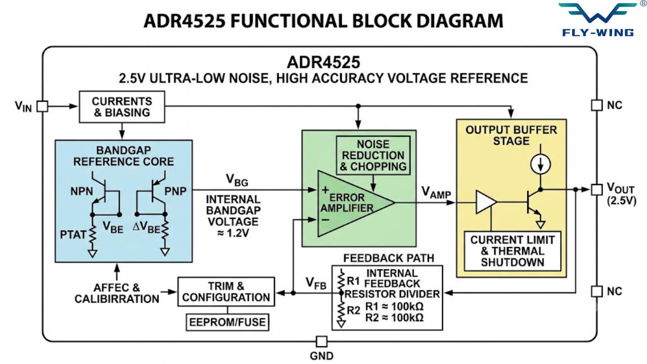
The ADR4525, which was developed by Analog Devices, is among the group of high-accuracy voltage references that have been designed specifically for this task. The device is part of the group of six fixed voltage references from the ADR45xx series.
Why Precision Voltage References Are Critical
Bandgap vs. Buried Zener: Two Competing Architectures
The two major types of circuitry used in designing voltage references are:
Band gap reference circuits. This type of circuit compensates for the temperature coefficient of the forward biased diode junction by matching it with a complementary voltage difference to provide a relatively low dependence of the output on the supply voltage compared to the other circuitry. Band gap references use lower supply voltages and consume lower amounts of power compared to the buried Zener references. In addition, the band gap references have greater stability than the buried Zeners. However, band gap output voltage has greater sensitivity to temperature; therefore, it must be compensated on chip.
Buried Zener references consist of Zener diode junctions buried beneath the silicon surface so as to avoid the stress and contamination problems of a normal surface Zener reference. Buried Zener references are not prone to large temperature drifts, but they need high minimum operating voltage of at least 5 V due to the 6.5 V required across the Zener breakdown region before adding temperature compensation diodes on top of it.
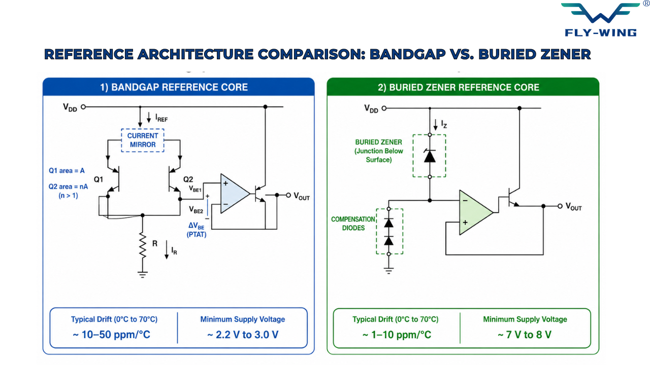
The ADR4525 employs a new bandgap-based core topology technology developed by Analog Devices that reportedly addresses the performance gap with respect to buried Zeners while retaining the benefits of low supply voltage and low power consumption in a bandgap configuration. This is the reason why the ADR4525 can run at just 3 V and still maintain 2 ppm/°C drift, which would otherwise only be possible with a buried Zener technology in previous generations of references.
Worked Example: The Real Cost of Reference Drift
Numbers make this clear. Assume a 16-bit ADC with a working range from commercial temperatures and calibrated at 25°C. In order to remain within ± one least significant bit over a 45°C temperature span using a 16-bit ADC, then the reference needs to have better than approximately 1 ppm/°C stability.
The numbers behind it: a 1 ppm/°C reference multiplied by a 5V output multiplied by 45°C gives you around 225 microvolts of drift. In the case of a 16-bit ADC with a 5V range, one LSB will equal about 76 microvolts. Drift of just 225 microvolts consumes almost 3 LSBs of your ADC’s total resolution, let alone the other effects like noise and nonlinearity of the ADC itself.
At 14-bit and 16-bit resolutions, the LSB shrinks to the microvolt range, and the internal reference’s drift, noise, and initial error become the dominant error source, often larger than the converter’s own quantization error. This is precisely the gap an external precision reference like the ADR4525 is designed to close.
It’s not a hypothetical issue. This is why all serious data acquisition devices, calibration equipment, and high-precision measuring products sold in the market utilize an external reference IC instead of using the internal reference available within the converter.
ADR4525 Electrical Specifications
The values below come from the Analog Devices ADR4520/ADR4525/ADR4530/ADR4533/ADR4540/ADR4550 datasheet, Revision G, dated May 2024. Always confirm exact figures against the current datasheet revision and your specific grade selection before finalizing a design.
Output Voltage and Initial Accuracy
The ADR4525 produces a constant 2.5 V output. The initial output tolerance is defined as ±0.02% max for grades B, C, and D, which balance price and accuracy. That represents an error of about ±0.5 mV from the 2.5 V nominal output, without taking into account any errors due to temperature changes.
Temperature Coefficient
Maximum temperature coefficient is specified at 2 ppm/°C for ADR4520, ADR4525, ADR4530, ADR4533, ADR4540, and ADR4550 families. Applying this figure to the example of Section 2.2, we can say that the drift due to temperature changes for ADR4525 will be around 225 microvolts for 2.5 V nominal output voltage across 45°C range of temperatures.
Output Noise and Long-Term Drift
Output noise from 0.1 Hz to 10 Hz is given at less than 1 µV peak-to-peak average, as determined on the VOUT of 2.048 V with the related part ADR4520, while the ADR4525 is built on the same low-noise architecture as ADR4520. Low-frequency output noise range is important since it falls into the measurement range which precise DC measuring equipment cares about – higher frequency noise can be easily filtered by the measurement system.
There is no power cycle hysteresis even when the device is powered down for around four hours and is powered on once again. It makes the product suitable for devices which need to preserve their accuracy after the power cycle.
Supply Voltage, Dropout, and Quiescent Current
Input voltage for the ADR4525 can be between 3 V and 15 V. The dropout voltage is 300 mV when the load current is 2 mA, and the output voltage exceeds 3 V. The maximum quiescent current is 950 microamps, which means that the chip does not have any effect on the current consumption of the entire battery powered circuit.
Output Current Capability
The output pin of the device can source and sink currents up to 10 mA each. That means the output stage of the chip is capable of driving directly reference pins of most ADCs and DACs without the need of any external buffer amplifiers. However, for reference inputs with transient current loads, the output capacitor becomes mandatory (see Section 6).
ADR4525 Pinout: Every Pin Explained
The ADR4525 is available in an 8-lead SOIC package. While the pin configuration is straightforward, there are certain pins such as NIC and DNC that tend to create confusion among designers, resulting in incorrect circuit design and connections at times.
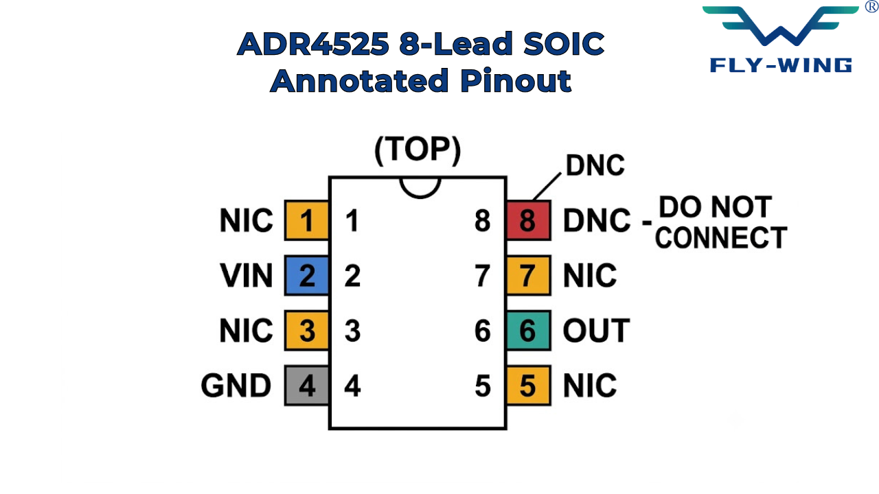
| Pin | Name | Function |
|---|---|---|
| 1 | NIC | Not Internally Connected — leave floating, may be tied to ground for PCB convenience |
| 2 | VIN | Supply voltage input (3 V to 15 V) |
| 3 | NIC | Not Internally Connected — leave floating, may be tied to ground for PCB convenience |
| 4 | GND | Ground — system reference |
| 5 | NIC | Not Internally Connected — leave floating, may be tied to ground for PCB convenience |
| 6 | OUT | Precision regulated output (2.5 V) — connect output capacitor here |
| 7 | NIC | Not Internally Connected — leave floating, may be tied to ground for PCB convenience |
| 8 | DNC | Do Not Connect — internally connected to a die node; connecting may degrade performance or cause damage |

VIN, GND, and OUT — The Three Pins That Matter
This circuit contains electrical function on only three pins: the VIN pin (pin 2), which receives the power supply voltage, the GND pin (pin 4), which receives the ground reference voltage, and the OUT pin (pin 6), which gives the regulated output voltage of 2.5V. This limited number of pins is characteristic for voltage reference ICs; there are no enable pins, no trim pins, and no connection for configuring the device.
NIC vs. DNC — Why the Difference Matters
NIC means Not Internally Connected, which means that the pins are not connected internally to the die at all. DNC means Do Not Connect, which means that the pin is connected internally to the die and should be left without any external connections. This is important since the NIC pins really are inactive and can safely be grounded for symmetry purposes if needed. On the other hand, the DNC pin will affect the internal trim/test circuits if it is made to carry a voltage and must therefore be left entirely untouched.
If your PCB layout software auto-routes unused pins to ground by default, manually exclude pin 8 from that rule before finalizing your board.
How the ADR4525 Works Internally
The Reference Core
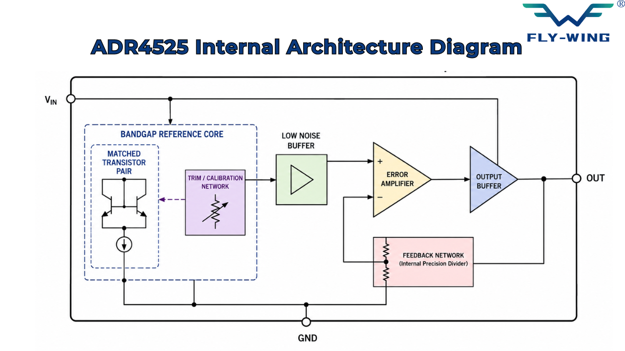
At the heart of the ADR4525 lies the production of a temperature-insensitive voltage based on the bandgap, which uses pairs of transistors while applying different currents to each pair. The difference in voltages measured at the base-to-emitter junction of these transistors has a known and characterized behavior with respect to absolute temperature. When you combine this temperature-dependent voltage with another voltage component that is independent of temperature in the right proportions, the circuit creates an output voltage that remains virtually insensitive to changes in temperature; this principle underlies every bandgap reference design.
The things that make the ADR4525 more than just a simple bandgap reference inside a typical microcontroller include precision laser trimming to account for differences between transistors, other temperature compensation networks, and careful placement of the components to prevent thermal gradients from being a source of additional errors.
Output Buffer and Load Regulation
However, the core voltage maintains a fixed value but exhibits high impedance; thus, it cannot accurately drive a load. The buffer amplifier takes the reference input in the form of core voltage and drives the output pin, providing low output impedance. The feedback system continually compares the output voltage with the reference and corrects the deviation in output voltage because of any change in load current.
The feedback system is responsible for the load regulation of the device; that is, it maintains output voltage constant even when the load current is changing from zero to the maximum 10 mA. It is because of this feedback system that capacitor selection at the output becomes an important issue since stability of the feedback system depends on the impedance presented by the capacitor as discussed in Section 6.2.
Power-Up Behavior and Thermal Hysteresis
One particular aspect of these devices is the total lack of hysteresis in the power cycling, even after several hours of powering down the circuit. While most reference ICs tend to show some kind of shift in the output voltage upon the very first power-on after a shutdown period, slowly returning to their original setpoint, the design of the ADR4525 completely eliminates this phenomenon, which holds crucial importance for any instrument that users turn on and off constantly between measurements.
ADR4525 Application Circuit: Basic Reference Connection
Minimal Working Circuit
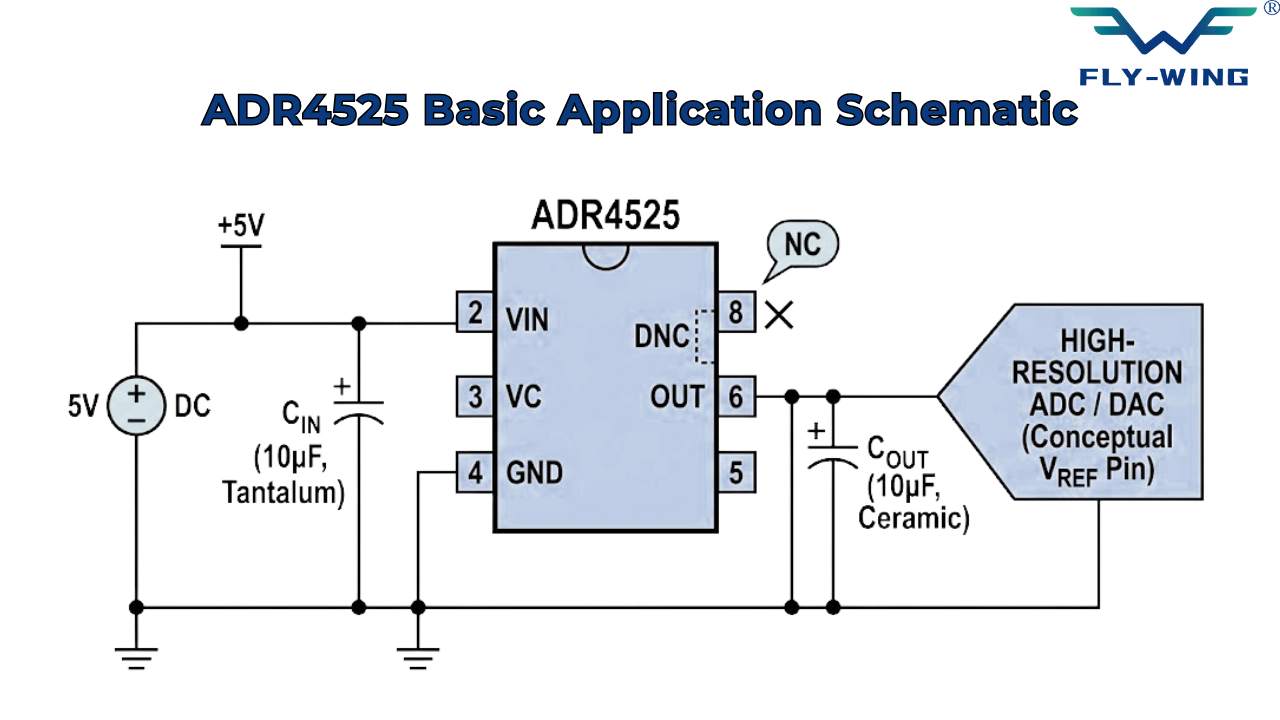
The basic application circuit for the ADR4525 requires remarkably few components: the IC itself, an input capacitor, an output capacitor, and the connections to your supply and your ADC or DAC’s reference pin.
- ADR4525 IC (8-lead SOIC)
- Input capacitor — typically 0.1 µF to 1 µF ceramic, placed close to the VIN pin
- Output capacitor — typically 1 µF to 10 µF ceramic, placed close to the OUT pin
- Connection from VIN to a clean, regulated supply rail (3 V to 15 V)
- Connection from OUT to your ADC or DAC’s VREF input pin
- Common ground reference between the ADR4525, the supply, and the converter
Input and Output Capacitor Selection
The input capacitor filters power supply noise prior to reaching the reference core, thereby lowering the likelihood of switching noise from the power supply coupling onto the output. A 0.1uF – 1uF ceramic capacitor located close to the VIN pin is adequate for most designs.
The output capacitor on the other hand stabilizes the output voltage during times of sudden load transient or load change when the connected ADC or DAC presents large current pulses for short periods of time as part of their conversion cycles, as well as providing additional noise filtering on the precision output itself. Manufacturers normally recommend a 1uF – 10uF ceramic capacitor, but check that the effective capacitance meets specification due to your actual operating DC bias. Ceramic capacitors, especially the smaller (X5R or X7R) dielectric types that engineers use extensively in compact designs tend to lose a measurable amount of their rated capacitance when you apply an increasing DC bias across them.
Before finalizing capacitor selection for a high-precision design, consult the load transient response and output impedance curves in the ADR4525 datasheet, and verify stability empirically on the bench with your actual chosen capacitor part number.
PCB Layout Guidelines
Minimize the trace lengths for the output capacitor placement close to the OUT and GND pins. Parasitic inductances caused by long traces can affect the transient response adversely. Connect the ground directly to the ground plane and not by connecting through other components’ ground pins because any voltage drop here would appear as an error in the reference voltage.
The thermal gradients between different parts of the package can also be a source of small errors in precise applications. This is because engineers designed the bandgap core of the device under the assumption that the temperature of the die remains constant. Do not locate heat generating components like resistors or high current paths next to the ADR4525 package.
ADR4525 Application Domains
Precision Data Acquisition Systems
This is the fundamental application scenario. If any data acquisition device uses a 14-bit, 16-bit, or even higher ADC, then it has to use some external reference to attain its full accuracy. As ADC resolution increases from 12-bit to 24-bit devices, the demands on stability with respect to temperature, noise, and drift also increase. This is precisely what the ADR4525 was designed for.
High-Resolution DAC Output Stages
Highly precise digital-to-analog converters depend just as much on the accuracy of their references as analog-to-digital converters, since the input code to the converter chooses the output voltage of a DAC as a proportion of the reference voltage. ADR4525 is the 2.5 V reference on the Analog Devices’ evaluation board for the AD5676R precision DAC.
Industrial Instrumentation and Calibration Equipment
The instruments used for calibration and industrial measuring systems have special requirements of the reference sensor because it should be able to maintain its accuracy for many years of operation, within a broad range of temperatures, and while undergoing power cycling before each measurement. This particular group of sensors exhibits a high resistance to thermal hysteresis and power cycle hysteresis. Thus, the absence of power cycle hysteresis allows extending the recalibration period of the equipment.
Portable and Battery-Powered Precision Equipment
With a maximum drop-out voltage of 300mV, this device can operate at a maximum current of 950µA making it an excellent choice for use within battery operated equipment since both product usability (battery life and the ability to maintain accurate regulation even at low final discharge voltages) depend on these factors.
ADR4525 vs. Family Variants and Alternatives
The ADR45xx Family
The ADR45xx family includes six types of fixed outputs. The six voltages are: ADR4520 (2.048 V), ADR4525 ( 2.5 V), ADR4530 (3.0 V), ADR4533 (3.3 V), ADR4540 (4.096 V), and ADR4550 (5.0 V). All members of this family have the same core design, accuracy grade, temperature coefficient specification, and 8-lead SOIC package; the only difference is in the voltage output.
| Part | VOUT (V) | Initial Acc. | TC (ppm/°C) | Notes |
|---|---|---|---|---|
| ADR4520 | 2.048 | ±0.02% | 2 max | Matches common 12-bit ADC ranges |
| ADR4525 | 2.5 | ±0.02% | 2 max | Most widely used — matches many ADC/DAC VREF defaults |
| ADR4530 | 3.0 | ±0.02% | 2 max | Matches 3V rail-referenced systems |
| ADR4533 | 3.3 | ±0.02% | 2 max | Matches 3.3V digital supply systems |
| ADR4540 | 4.096 | ±0.02% | 2 max | Common in 12-bit binary-friendly scaling |
| ADR4550 | 5.0 | ±0.02% | 2 max | Full-scale 5V systems, higher noise floor in absolute terms |
Choosing one of the family members should not be difficult; just make sure that the output voltage corresponds to what your particular ADC or DAC requires as the reference input voltage. The choices of 2.048 V and 4.096 V voltages are preferred for binary scaling to simplify further calculations in digital circuitry; 2.5 V and 5.0 V voltages correspond to standard reference inputs for ADCs/DACs.
Grade Selection: B, C, and D
Each family member can be purchased at different accuracies, usually classified as B, C, or D, with B being the most accurate guaranteed initial accuracy and D the least (and lowest-cost) grade. The temperature coefficient tolerance can also be somewhat different depending upon grade for some family members. When designing with a large error margin, the D grade might prove to be all that you require; when you require the most precise measurement, the B grade is worth every penny.
ADR4525W — The Automotive-Qualified Variant
Analog Devices also offers the ADR4525W in the same 8-lead SOIC package. Because engineers designed this variant for automotive applications, it passes the additional manufacturing and qualification tests required for automotive parts, such as AEC-Q100 procedures. Select this version if your final product demands automotive qualifying data. For any other application apart from automotive, you should select the regular part.
When to Consider a Buried Zener Reference Instead
Engineers usually choose bandgap references for applications requiring up to 12 bits of resolution, while tougher requirements rely on more accurate buried Zener references. However, newer bandgap designs like the ADR4525 significantly narrow this performance gap, making this general rule less absolute today. For 24-bit systems or applications requiring minimal drift over years of operation, a buried Zener reference still delivers better results.
Troubleshooting Common ADR4525 Problems
Output Voltage Unstable or Oscillating
The output capacitor is usually the culprit for oscillation problems. The oscillation can either be very slight in the case of mild ringing or it could be substantial enough to cause sustained oscillation during load transients. You can start by placing a ceramic capacitor between the OUT pin and GND pin; try using a value between 1 microfarad and 10 microfarads. If there is already a ceramic capacitor in place, refer to the device’s datasheet stability curve to see if it has an ESR specification that meets the feedback loop requirements.
Output Voltage Error Larger Than Expected
The following should be done in sequential order. First, make sure that the load current requirement falls within the ±10mA tolerance of the device – any higher than this will take the part beyond its rated accuracy specifications. Second, verify that the input voltage has sufficient headroom relative to the output voltage, taking into account the 300mV dropout specification – if the input drops below the required level relative to the output, the device will go out of regulation. Third, verify the board’s actual accuracy grade—substituting a specified B-grade part with a D-grade part increases error.
Excess Noise Appearing in Measurement Results
If downstream noise levels exceed reference specifications, insufficient decoupling or poor PCB layout often couples digital switching noise onto the OUT pin or its associated trace. When this happens, verify that you have mounted the output capacitor as close to the OUT pin as possible, route the ground connection to a solid ground plane, and check whether any high-speed digital traces run parallel or perpendicular to the reference output trace. Physically separating the high-speed digital traces from the reference output trace or routing a ground guard trace adjacent to the digital traces will help solve the coupling problems.
Verifying Reference Accuracy
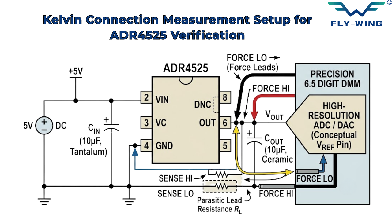
In order to confirm whether the real output voltage matches the specified one, apply a precise digital multimeter with at least 6.5 digits accuracy and preferably the four-wire measuring method in order not to make an error due to the leads resistance. Before making the reading, give some time for the unit to stabilize thermally, because the self-heating effect of the DMM itself, although minor, along with the ambient temperature stabilization can influence the reading in the beginning.
Frequently Asked Questions
The ADR4525 is a precision voltage reference IC that provides a stable 2.5 V output for high-accuracy analog systems. It improves the performance of ADCs and DACs by supplying a low-noise, temperature-stable reference voltage.
Internal references are suitable for basic applications but often lack the accuracy, low noise, and stability needed for high-resolution converters. The ADR4525 delivers much better precision for 14-bit, 16-bit, and higher-resolution ADCs.
NIC (Not Internally Connected) pins have no electrical connection to the die, and you may leave them floating or connect them to ground if you need to for PCB layout. Do not confuse them with DNC pins, which must remain unconnected.
The ADR4525 provides more than a fixed 2.5 V voltage reference—it preserves measurement accuracy in high-performance analog systems through its precision design. Always verify the capacitor’s effective capacitance under DC bias and follow the datasheet’s stability recommendations.
Choose the version that matches your ADC or DAC reference voltage requirement. The ADR4525 provides a 2.5 V output, while the ADR4550 provides a 5.0 V output with similar performance characteristics.
Yes. Its low quiescent current and 300 mV dropout voltage make it a good choice for battery-powered precision instruments while maintaining accurate regulation as battery voltage decreases.
Conclusion
The ADR4525 precision voltage reference provides more than a fixed 2.5 V voltage reference—it preserves measurement accuracy in high-performance analog systems through its precision design. With its low initial error, 2 ppm/°C maximum temperature coefficient, ultra-low output noise, low dropout voltage, and zero power-cycle hysteresis, it provides the stable reference required by high-resolution ADCs, DACs, industrial instrumentation, and battery-powered precision equipment.
Selecting the correct output voltage variant, following the recommended capacitor values, and implementing proper PCB layout practices are just as important as choosing the device itself. The ADR4525 delivers reliable long-term stability and repeatable performance when engineers follow these design guidelines, making it an excellent choice for applications where every microvolt of accuracy matters.

COMMENTS