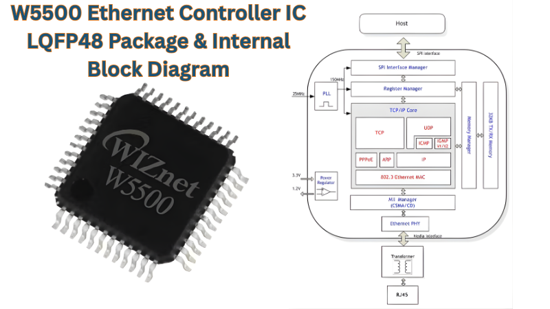
What Is the W5500 Ethernet Controller IC?
The W5500 Ethernet Controller IC is a hardwired TCP/IP embedded Ethernet controller from WIZnet. It combines a complete TCP/IP stack, a 10/100 Ethernet MAC, and a PHY in a single chip. It provides a means of direct Internet connection for microcontrollers through a high-speed SPI interface running at up to 80 MHz. Instead of running a software stack on the host microcontroller unit, the W5500 performs all TCP/IP processing using dedicated hardware. It provides deterministic and reliable network operation at the firmware level.
In practice, this architectural difference makes a substantial impact on the manner in which an Arduino or STM32 communicates with the W5500; in fact, the communication is done in the same way as accessing any other SPI-type device through reading and/or writing registers. The W5500 does all framing, acknowledgments, retransmissions, and ARP resolution independently. Once the host MCU issues a SEND command, the W5500 takes care of delivering a verified TCP segment to the network.
Supported Hardwired Protocols
All of the protocols TCP, UDP, ICMP, IPv4, ARP, IGMP, and PPPoE are implemented in the W5500 hardware alone. One design specification that engineers need to consider when dealing with large payloads is that the W5500 does not support IP fragmentation. In addition, there is currently no support for IPv6, and all IPv6 functionality will be handled by the successor IC (W6100).
Feature Highlights
- 8 independent sockets — Every socket serves as a TCP/UDP connection with it is own register space, TX buffer, RX buffer. All 8 sockets can be enabled at the same time. So you can run protocols concurrently such as MQTT, HTTP, Modbus TCP and DNS, all at the same time.
- 32 KB configurable buffer memory — The total memory space allocated to TX/RX buffers is divided evenly across sockets at 1 KB increments based on the value of Sn_TXBUF_SIZE and Sn_RXBUF_SIZE register settings. A design requiring one high speed socket can allocate up to 16 KB of memory and utilize the balance of the memory for other sockets.
- 5V I/O signal tolerance — All SPI and digital I/O pins (GPIOs) are designed to accept 5V logic levels which allows for direct connections to existing 5V based Arduino and AVR systems without the need for any level converting hardware.
- Wake on LAN (WOL) via Magic Packet over UDP — The chip can wake from power-down mode on receipt of a standard Magic Packet, reducing idle power consumption to approximately 0.6 mA.
- LED outputs — There are several indicators with open drain outputs that can be used to indicate whether they are operating in full or half duplex mode, link status, speed (10 vs. 100), and active status. In most cases, these indicators are directly connected to commonly available LED’s through a series current limiting resistor.
- Power-down mode — reduces operating current significantly for battery-powered or energy-harvesting IoT nodes.
Why Engineers Choose the W5500 Over a Software Stack
Software-based TCP/IP stacks such as lwIP running on an STM32 consume valuable MCU cycles, SRAM, and flash. Interrupt-based packet processing can interfare with application code execution. Stack usage can differ depending on the load. The W5500 eliminates all such issues. Engineers can use the W5500 for networking using simple socket commands over an SPI bus. Engineers can read and write registers and data buffers directly. There is no IP stack library to port, optimize, and debug. This is the main reason why the W5500 has remained the undisputed leader in resource-constrained embedded Ethernet solutions for over a decade in production environments.
The W5500 is suitable for wired IoT sensor networks, industrial control system controllers, serial-to-Ethernet converters, remote I/O devices, building automation gateways, and all other applications where wireless RF connectivity is either unavailable or unreliable.
Note on throughput: The PHY of the W5500 is rated for 100 Mbps, the actual TCP throughput is limited by the speed of the SPI interface, as well as the socket buffer management strategy, rather than the PHY speed. The actual measured performance figures, as well as the factors affecting them, are covered in (SPI Performance & Throughput).
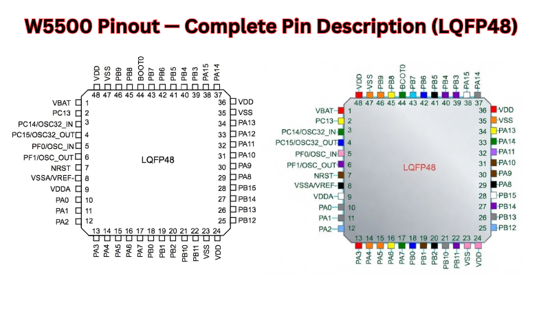
A solid understanding of the W5500 pinout is a fundamental prerequisite for correct schematic capture, PCB layout, as well as firmware bring-up. Any incorrect connections, e.g., a swap of MOSI/MISO, a lack of a connection for the TOCAP, or a floating state for the EXRES1, can cause a lack of SPI response or a flaky PHY link. This section lists all 48 pins from the official WIZnet Datasheet v1.1.0, grouped by functional category, with important notes extending beyond the information provided within the datasheet table.
W5500 Pinout — Complete Pin Description (LQFP48)
Package Overview & Pin Orientation
The W5500 Ethernet Controller IC is housed in a 48-pin lead-free package with an LQFP footprint. The dimensions are 7×7 mm with a 0.5 mm pin pitch. It is important to understand that there is no QFN package for the W5500. This is a common error found in the datasheets of third-party sources, which is actually a legacy of the W5200 IC. All footprint and land pattern design must be based on the dimensions of the LQFP48 package as defined in Datasheet v1.1.0.
Pin numbering convention: Pin 1 is located at the top-left corner of the IC (marked with a dot or a chamfer on the package). The numbering of the pins is done clockwise when viewed from above. The sides are defined as follows:
PHY Analog Interface Pins (Pins 1–11)
These pins directly interface with the Ethernet magnetics (isolation transformer). These are analog differential signals, and these signals need to be routed as differential pairs of matched length. No digital signals should be routed close to these signals.
Analog Bias & Internal Regulator Pins (Pins 12–22)
These pins support the internal analog bias circuits and the on-chip 1.2V regulator. They require specific external passive components — omitting them is a guaranteed path to chip instability or no-start behavior.
Reserved Pins (Pin 23, Pins 38–42)
Pin 23 and pins 38–42 are marked RSVD (Reserved) in the datasheet and include an internal pull-down bias. They must connect to ground and must not be left floating, nor connected to any signal or power supply.
If you violate this requirement it can cause the device to enter an undefined state of operation which could cause the device to behave unpredictably or not function correctly.
LED Output Pins (Pins 24–27)
There are four dedicated pins for LEDs, which are SPDLED (Speed), LINKLED (Link), DUPLED (Duplex), and ACTLED (Activity). The LEDs are open-drain, active-low type. The LEDs must be connected with a current restriction resistor, which is generally 330 Ω for normal 3 mA LEDs, to the 3.3 V supply rail. The resistor is used to restrict the current, with the positive end of the LED connected to the junction point of the resistor and the negative end of the LED connected to the W5500 pin.
Design note: All four LED pins can be left unconnected if status LEDs are not required. If using a combo RJ45 module with integrated LEDs (e.g., HR911105A), check whether the module’s internal LEDs are driven by the magnetics side or need external connection to these pins. Do not rely on module LEDs without verifying the schematic.
Digital Power & Ground (Pins 28–29)
Crystal & Clock Input Pins (Pins 30–31)
The W5500 requires a 25 MHz reference clock for its PHY. Two options exist:
Crystal circuit requirements:
- Fundamental mode 25 MHz Crystal, with load capacitance specified by the crystal manufacturer (18-22pF).
- The load capacitors should be connected between both XI and XO terminals to GND, as close to the crystals as possible (within 3 mm).
- A guard ring should be formed around the traces carrying the crystals, together with a GND ring connected to GND plane.
- No other signal traces should be routed under or near the crystal circuit.
SPI Interface Pins (Pins 32–35)
The W5500 SPI interface consists of four pins: SCSn (chip select, active low), SCLK (clock input), MISO (output from W5500 to host), and MOSI (input from host to W5500).
Control & Interrupt Pins (Pins 36–37)
Reset timing requirements summary:
PHY Mode Selection Pins (Pins 43–45)
Pins PMODE0, PMODE1, and PMODE2 determine the PHY operating mode at power-on reset. All three have internal pull-ups. The default hardware state (all three floating/pulled high: 111) enables all speeds with auto-negotiation — the correct setting for the vast majority of designs.
PMODE[2:0] Configuration Table:
Complete Pin Reference Table
The table below is the authoritative pin reference for schematic capture.
SPI Interface & Communication Protocol of W5500 Ethernet Controller IC
The SPI interface is used as the single point of contact between the host MCU and all functions offered by the W5500 IC, including hardware TCP/IP, sockets, networking, and buffer access functions. Knowledge of the SPI protocol of the W5500 is therefore a must, as this forms the basis of all firmware developed for this IC.
The SPI interface of the W5500 IC is differentiated from other ICs that offer a simple SPI interface for their registers in that it follows a specific three-phase frame format for all its operations, whether it is a single byte write operation for a configuration byte or a full-length write of a TCP payload into the TX buffer. A good understanding of this format at a bit level is necessary to avoid the most common class of W5500 IC bring-up problems.
SPI Operating Modes of W5500 Ethernet Controller IC
The W5500 supports SPI Mode 0 (CPOL=0, CPHA=0) and SPI Mode 3 (CPOL=1, CPHA=1). In both modes, data is sampled on the rising edge of SCLK and shifted out on the falling edge. The distinction is only the idle state of SCLK: LOW in Mode 0, HIGH in Mode 3.
Implementation note: Most microcontroller SPI peripherals are in Mode 0 by default. Unless you have a specific reason for choosing Mode 3, such as sharing a bus with a Mode 3 device, set your host MCU SPI to Mode 0 and keep SCLK low when idle. Mixing SPI modes on a shared bus without control of chip select will corrupt every transaction on that bus.
VDM and FDM are two SPI data modes supported by W5500: In Variable Length Data Mode, the host controls the length of the data frame with SCSn; in Fixed Length Data Mode, the length is fixed at 1, 2, or 4 bytes, depending on OM bits 1 and 0, respectively. VDM is recommended for standard usage, while FDM is available for use when the host cannot independently control SCSn, and WIZnet strongly advises against its use unless no alternative is possible.
SPI Frame Format — The 3-Phase Structure
This is the most technically critical section for any engineer implementing W5500 Ethernet Controller IC firmware from scratch. Every W5500 SPI transaction consists of exactly three phases: a 16-bit Address Phase, an 8-bit Control Phase, and an N-byte Data Phase.
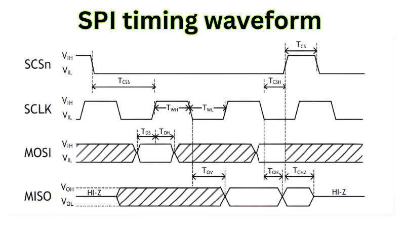
Phase 1 — Address (16 bits, MSB first)
The Address Phase specifies the 16-bit offset address of the target register or memory location in the selected block. The 16-bit offset address value is transmitted in a sequence from the most-significant bit.
Key points engineers frequently misunderstand:
- The address is a relative offset address in a block rather than an absolute memory address. The address 0x0009 represents a register offset 0x0009 in a block selected by BSB bits in Phase 2.
- The W5500 automatically increments the address by 1 for sequential (burst) reads or writes in the Data Phase. Therefore, no address phase is required for a sequential access for each byte.
- The same address 0x0000 exists in many blocks and represents different registers according to the selected block by BSB.
Phase 2 — Control Byte (8 bits)
The 8-bit Control Phase is composed of Block Select bits BSB[4:0] in bits 7–3, the Read/Write Access Mode bit RWB in bit 2, and SPI Operation Mode bits OM[1:0] in bits 1–0.
Bit: [7] [6] [5] [4] [3] [2] [1] [0]
|——BSB[4:0]——| RWB |–OM–|
BSB[4:0] — Block Select Bits (bits 7–3):
The Block Select bits select the target register or memory block to which the offset address set in the Address Phase belongs.
Critical: Any BSB value listed as Reserved in the datasheet will cause W5500 malfunction if used. Do not derive BSB values by arithmetic shortcuts without verifying against the datasheet table.
RWB — Read/Write Access Mode Bit (bit 2):
OM[1:0] — Operation Mode Bits (bits 1–0):
For all standard firmware using VDM, OM[1:0] is always 00.
Worked example — building a control byte:
To write to the Socket 0 TX Buffer at address offset 0x0040:
- BSB = 00010 (Socket 0 TX Buffer)
- RWB = 1 (Write)
- OM = 00 (VDM)
- Control byte = 0b00010_1_00 = 0x14
To read from Common Registers at address 0x0039 (VERSIONR):
- BSB = 00000 (Common Registers)
- RWB = 0 (Read)
- OM = 00 (VDM)
- Control byte = 0b00000_0_00 = 0x00
Phase 3 — Data (N bytes, MSB first)
In VDM mode, the length of the SPI data phase is controlled by the SCSn control signal. The data phase may be from 1 byte up to N bytes depending on when the host deasserts SCSn. Each byte is sent in the order of the most significant bit first (MSB first).
The auto-increment behavior is the basis for efficient burst operations:
- Burst write: Assert SCSn → send Address → send Control (RWB=1) → clock out bytes 1 through N on MOSI → deassert SCSn. The W5500 writes byte 1 to the base address, byte 2 to base+1, byte 3 to base+2, and so on
- Burst read: Assert SCSn → send Address → send Control (RWB=0) → clock N bytes on MISO → deassert SCSn. The W5500 outputs data from base address through base+N-1
This burst capability is critical for throughput. Writing a 1460-byte TCP payload to the TX buffer in a single burst transaction (one SCSn assertion) is dramatically more efficient than 1460 individual single-byte SPI transactions.
Register Map & Memory Organization
The W5500 Ethernet Controller IC address space is organized into logically separate blocks, each selected by the BSB field in the Control Phase. Understanding this organization is prerequisite to correctly constructing every SPI frame.
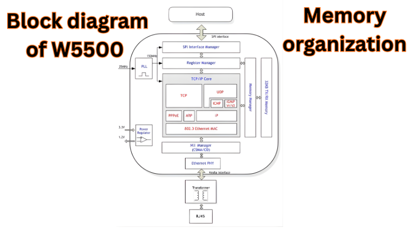
Common Register Block (BSB = 00000)
The Common Register block contains all global configuration registers including the Mode Register (MR), Gateway Address (GAR), Subnet Mask (SUBR), Source Hardware Address (SHAR), Source IP Address (SIPR), interrupt registers, retry time, PHY configuration, and the chip version register (VERSIONR).
| Address | Register | Width | Access | Description |
|---|---|---|---|---|
| 0x0000 | MR | 1 byte | R/W | Mode Register — software reset (bit 7), PPPoE, ping block |
| 0x0001–0x0004 | GAR | 4 bytes | R/W | Gateway IP Address (e.g., 192.168.1.1) |
| 0x0005–0x0008 | SUBR | 4 bytes | R/W | Subnet Mask (e.g., 255.255.255.0) |
| 0x0009–0x000E | SHAR | 6 bytes | R/W | Source MAC Address (must be unique per device) |
| 0x000F–0x0012 | SIPR | 4 bytes | R/W | Source IP Address |
| 0x0013–0x0014 | INTLEVEL | 2 bytes | R/W | Interrupt Assert Wait Time |
| 0x0015 | IR | 1 byte | R/W | Interrupt Register — global interrupt flags |
| 0x0016 | IMR | 1 byte | R/W | Interrupt Mask Register |
| 0x0017 | SIR | 1 byte | R | Socket Interrupt Register — which socket raised interrupt |
| 0x0018 | SIMR | 1 byte | R/W | Socket Interrupt Mask Register |
| 0x0019–0x001A | RTR | 2 bytes | R/W | Retry Time (default 0x07D0 = 200 ms) |
| 0x001B | RCR | 1 byte | R/W | Retry Count (default 8 retries) |
| 0x002E | PHYCFGR | 1 byte | R/W | PHY Configuration — link status, speed, duplex, reset |
| 0x0039 | VERSIONR | 1 byte | R | Chip version — always reads 0x04 on W5500 |
Socket Register Block (BSB = 00001 / 00101 / … per socket)
Each of the 8 sockets has its own independent register block. All socket registers share the same offset address layout; the BSB value selects which socket’s registers are accessed.
| Offset | Register | Width | Description |
|---|---|---|---|
| 0x0000 | Sn_MR | 1 byte | Socket Mode — set protocol (TCP=0x01, UDP=0x02, MACRAW=0x04, IPRAW=0x03, …) |
| 0x0001 | Sn_CR | 1 byte | Socket Command — OPEN, LISTEN, CONNECT, DISCON, CLOSE, SEND, RECV, SEND_KEEP, etc. |
| 0x0002 | Sn_IR | 1 byte | Socket Interrupt — CON, DISCON, RECV, TIMEOUT, SEND_OK flags (write 1 to clear) |
| 0x0003 | Sn_SR | 1 byte | Socket Status — SOCK_CLOSED, SOCK_INIT, SOCK_LISTEN, SOCK_ESTABLISHED, SOCK_CLOSE_WAIT, etc. |
| 0x0004–0x0005 | Sn_PORT | 2 bytes | Source port number for this socket |
| 0x000C–0x000F | Sn_DIPR | 4 bytes | Destination IP Address (TCP: connect target; UDP: send target) |
| 0x0010–0x0011 | Sn_DPORT | 2 bytes | Destination port number |
| 0x001E | Sn_TXBUF_SIZE | 1 byte | TX buffer size in KB (0=0KB, 1=1KB, 2=2KB, 4=4KB, 8=8KB, 16=16KB) |
| 0x001F | Sn_RXBUF_SIZE | 1 byte | RX buffer size in KB (same valid values as Sn_TXBUF_SIZE) |
| 0x0020–0x0021 | Sn_TX_FSR | 2 bytes | TX Free Size Register — bytes available to write |
| 0x0022–0x0023 | Sn_TX_RD | 2 bytes | TX Read Pointer (managed by W5500 chip) |
| 0x0024–0x0025 | Sn_TX_WR | 2 bytes | TX Write Pointer (managed by host firmware) |
| 0x0026–0x0027 | Sn_RX_RSR | 2 bytes | RX Received Size Register — bytes available to read |
| 0x0028–0x0029 | Sn_RX_RD | 2 bytes | RX Read Pointer (managed by host firmware) |
| 0x002A–0x002B | Sn_RX_WR | 2 bytes | RX Write Pointer (managed by W5500 chip) |
Socket TX & RX Buffer Blocks of W5500 Ethernet Controller IC
Each socket has two dedicated buffer blocks — TX and RX — addressed by their respective BSB values. The physical buffer space totals 32 KB, shared across all 8 sockets. Buffer allocation is configured via Sn_TXBUF_SIZE and Sn_RXBUF_SIZE registers before the socket is opened.
| Allocation Strategy | Use Case / Typical Application |
|---|---|
|
All 8 sockets: 2 KB TX + 2 KB RX each (Total: 16 KB TX + 16 KB RX) |
Balanced multi-socket applications • 4 TCP + 4 UDP sockets • General-purpose IoT / multiple clients • Moderate throughput per connection |
|
Socket 0: 16 KB TX + 16 KB RX Sockets 1–7: 0 KB TX + 0 KB RX (Total: 16 KB TX + 16 KB RX) |
Maximum single-socket throughput • Large file transfer (HTTP/FTP download/upload) • High-speed streaming (one direction) • Bulk data logger / backup |
|
Socket 0: 8 KB TX + 8 KB RX Sockets 1–3: 4 KB TX + 4 KB RX each Sockets 4–7: 1 KB TX + 1 KB RX each (Total: 8 + 3×4 + 4×1 = 24 KB TX / RX — requires 32 KB chip) |
Mixed priority allocation • One high-bandwidth channel (e.g. firmware update, video stream) • Several medium-priority control sockets • Low-priority monitoring / heartbeat sockets • Typical in industrial |
|
Socket 0: 8 KB TX + 8 KB RX Socket 1: 4 KB TX + 4 KB RX Sockets 2–7: 1 KB TX + 1 KB RX each (Total: 8 + 4 + 6×1 = 18 KB TX / RX) |
Common practical compromise • Primary high-speed socket • One secondary reliable channel • Multiple lightweight MQTT |
|
Socket 0–3: 4 KB TX + 4 KB RX each Sockets 4–7: 0 KB (Total: 16 KB TX + 16 KB RX) |
Moderate multi-connection server • Up to 4 simultaneous TCP clients • Web server + configuration + OTA + logging |
SPI Initialization Sequence
This is the most-searched PAA target for this topic and requires the highest precision. The sequence below is verified against WIZnet ioLibrary_Driver source code and the official datasheet.
Step 1 — Hardware Reset
Assert RSTn LOW for a minimum period of 500 µs (it is recommended to use a 1 ms period to have some margin). Then make it HIGH. Wait 50 ms before any SPI access is attempted. This allows the internal PLL, PHY, and the 25 MHz crystal oscillator to settle. Not waiting long enough is the most common cause of initialization failure in environments where the firmware restarts without power-cycling the device.
// Bare-metal C example

GPIO_ResetPin(W5500_RST_PIN);

delay_ms(1);

GPIO_SetPin(W5500_RST_PIN);

delay_ms(50);  // Wait for PLL + PHY stabilization
Step 2 — Verify Chip Identity
Read VERSIONR (Common Register, offset 0x0039). The returned value must be 0x04. Any other value — including 0x00 or 0xFF — means the SPI bus is not communicating correctly. Do not proceed with configuration if this check fails.
// SPI transaction: BSB=00000, RWB=0, OM=00

// Address: 0x0039, Control: 0x00

uint8_t version = w5500_read_byte(0x0039, 0x00);  // Returns 0x04

if (version != 0x04) { /* SPI error — halt and debug */ }
Step 3 — Write MAC Address (SHAR)
Write the 6-byte MAC address to SHAR (Common Register offsets 0x0009-0x000E) using a burst write. Every device connected to a network should have a unique MAC address. The OUI prefix for all WIZnet devices is 00:08:DC. You can use this as a prefix for all WIZnet-based devices, or create a locally administered MAC address by setting bit 1 in the first byte to 1.
uint8_t mac[6] = {0x00, 0x08, 0xDC, 0x01, 0x02, 0x03};

// Burst write: Address=0x0009, Control=BSB(00000)|RWB(1)|OM(00) = 0x04

w5500_write_burst(0x0009, 0x04, mac, 6);
Step 4 — Write Network Configuration
Write Gateway IP (GAR, 0x0001–0x0004), Subnet Mask (SUBR, 0x0005–0x0008), and Source IP (SIPR, 0x000F–0x0012) in sequence. All are burst writes to the Common Register block (BSB = 00000, RWB = 1).
uint8_t gateway[4] = {192, 168, 1, 1};

uint8_t subnet[4]  = {255, 255, 255, 0};

uint8_t ip[4]      = {192, 168, 1, 100};

w5500_write_burst(0x0001, 0x04, gateway, 4);  // GAR

w5500_write_burst(0x0005, 0x04, subnet,  4);  // SUBR

w5500_write_burst(0x000F, 0x04, ip,      4);  // SIPR
Step 5 — Allocate Socket Buffer Memory
For each socket that will be used, set Sn_TXBUF_SIZE (offset 0x001E) and Sn_RXBUF_SIZE (offset 0x001F) in the socket’s register block. The default after reset is 2 KB per socket per direction (2 × 8 sockets = 16 KB per direction). Only change if a non-default allocation is needed.
// Example: give Socket 0 a 4KB TX and 4KB RX buffer

// Socket 0 Register block: BSB = 00001 → control = 0x0C for write

w5500_write_byte(0x001E, 0x0C, 4);  // Sn_TXBUF_SIZE = 4 KB

w5500_write_byte(0x001F, 0x0C, 4);  // Sn_RXBUF_SIZE = 4 KB
Step 6 — Configure Socket Mode
Write the desired protocol to Sn_MR (offset 0x0000 in the socket register block).
Step 7 — Open the Socket
Write 0x01 (OPEN command) to Sn_CR (offset 0x0001 in the socket register block). After the OPEN command, poll Sn_SR (offset 0x0003) until it returns the expected status:
w5500_write_byte(0x0001, 0x0C, 0x01);  // Sn_CR = OPEN

// Poll Sn_SR until socket is ready

uint8_t status;

do {

    status = w5500_read_byte(0x0003, 0x08);  // Read Sn_SR

} while (status != 0x13);  // Wait for SOCK_INIT (TCP)
Important: The W5500 clears Sn_CR automatically after processing a command. Do not write the next command until Sn_CR reads back as 0x00. Polling Sn_CR for 0x00 between commands is the correct production implementation pattern.
Complete SPI Read & Write Function Reference (Bare-Metal C)
The following functions represent the minimum correct implementation of W5500 SPI access in bare-metal C. All higher-level socket operations are built on these two primitives.
/**

 * W5500 SPI write — single byte, VDM mode

 * @param addr   16-bit offset address within selected block

 * @param ctrl   Control byte: BSB[4:0] | RWB=1 | OM=00

 * @param data   Byte to write

 */

void w5500_write_byte(uint16_t addr, uint8_t ctrl, uint8_t data) {

    CS_LOW();                       // Assert SCSn

    SPI_Transfer(addr >> 8);        // Address Phase: high byte

    SPI_Transfer(addr & 0xFF);      // Address Phase: low byte

    SPI_Transfer(ctrl | 0x04);      // Control Phase: force RWB=1 (write)

    SPI_Transfer(data);             // Data Phase: 1 byte

    CS_HIGH();                      // Deassert SCSn — marks frame end in VDM

}

/**

 * W5500 SPI read — single byte, VDM mode

 * @param addr   16-bit offset address within selected block

 * @param ctrl   Control byte: BSB[4:0] | RWB=0 | OM=00

 * @return       Byte read from W5500

 */

uint8_t w5500_read_byte(uint16_t addr, uint8_t ctrl) {

    uint8_t result;

    CS_LOW();

    SPI_Transfer(addr >> 8);        // Address Phase: high byte

    SPI_Transfer(addr & 0xFF);      // Address Phase: low byte

    SPI_Transfer(ctrl & ~0x04);     // Control Phase: force RWB=0 (read)

    result = SPI_Transfer(0x00);    // Data Phase: clock out dummy byte, capture MISO

    CS_HIGH();

    return result;

}

/**

 * W5500 SPI burst write — N bytes, VDM mode

 * @param addr   Base 16-bit offset address

 * @param ctrl   Control byte: BSB[4:0] | RWB=1 | OM=00

 * @param data   Pointer to source buffer

 * @param len    Number of bytes to write

 */

void w5500_write_burst(uint16_t addr, uint8_t ctrl,

                       const uint8_t *data, uint16_t len) {

    CS_LOW();

    SPI_Transfer(addr >> 8);

    SPI_Transfer(addr & 0xFF);

    SPI_Transfer(ctrl | 0x04);      // RWB=1

    for (uint16_t i = 0; i < len; i++) {

        SPI_Transfer(data[i]);      // W5500 auto-increments address each byte

    }

    CS_HIGH();                      // SCSn deassert terminates VDM burst

}
MicroPython equivalent (Raspberry Pi Pico / RP2040):
MicroPython’s network.WIZNET5K() driver wraps all three phases internally. Engineers using MicroPython do not need to implement these primitives manually — the machine.SPI() bus and network.WIZNET5K(spi, cs, rst) constructor handle frame construction automatically. Refer to Section 5.3 for the full MicroPython initialization example.
W5500 in IoT Applications
The benefit of the W5500 architecture, with its hardwired TCP/IP stack that operates independently of the host MCU, is best utilized in IoT applications. This section describes the three most common IoT application scenarios that make use of the W5500 Ethernet Controller IC: wired gateway architecture, the use of MQTT with a persistent TCP connection, and Modbus/TCP for industrial automation..
W5500 as a Wired IoT Gateway
Engineers choosing between Wi-Fi and wired Ethernet have a common practical difficulty. There are trade-offs with Wi-Fi: it has variable latency, RF interference from other devices communicating on the same channel, and a software TCP/IP stack that competes with an application for runtime on the CPU. The use of an Ethernet connection provides a stable and high-speed connection necessary for the real-time processing and communication required in IoT applications. In IoT applications requiring very high reliability and very low latency, using Ethernet has many advantages over using Wi-Fi.
Specifically, the W5500 Ethernet Controller IC meets these requirements. The chip is able to offload all processing for TCP/IP to its hardwired silicon so the host MCU can be used by the application to read sensors, perform control logic, or schedule RTOS tasks. This is the correct architecture for any gateway whose embedded application must support multiple parallel network sessions at the same time without degrading the MCU performance.
Practical socket allocation for a multi-protocol IoT gateway:
All six sessions above run concurrently. The W5500 Ethernet Controller IC handles all TCP state machines, retransmissions, and ARP resolution autonomously. The host MCU only processes application data.
Target application environments where W5500 wired Ethernet outperforms Wi-Fi:
- Factory floor sensor nodes in an environment where 2.4 GHz RF is congested by motor drive and welding equipment.
- Building automation controllers that require 24/7 uptime and need to avoid RF association failures.
- Medical monitoring equipment that is subject to wireless frequency restrictions.
- PLC to Cloud Gateways in Industrial Automation where network determinism is a compliance requirement.
MQTT over TCP with W5500 Ethernet Controller IC
The MQTT protocol is currently dominant in the application layer of IoT networks, fitting very well into the TCP socket model of the W5500 Ethernet Controller IC. When an MCU is integrated with the W5500, sensor readings can be sent, control commands received, dashboard information updated, data logged, and automation devices controlled over a reliable wired Ethernet network.
How MQTT maps to the W5500 socket model:
MQTT requires a persistent TCP connection between the client (the embedded device) and the broker (cloud server). On the W5500, this maps to a single socket configured in TCP client mode. The application layer sends and receives raw byte payloads; the W5500 Ethernet Controller IC handles all TCP framing, ACK, and retransmission transparently.
Socket configuration for MQTT:
// Socket 0 — TCP Client mode for MQTT

w5500_write_byte(Sn_MR, BSB_S0_REG, 0x01);    // Sn_MR = TCP mode

// Write broker IP to Sn_DIPR (e.g., 192.168.1.200)

uint8_t broker_ip[4] = {192, 168, 1, 200};

w5500_write_burst(Sn_DIPR, BSB_S0_REG, broker_ip, 4);

// Write broker port to Sn_DPORT

// Port 1883 = 0x075B (unencrypted MQTT)

// Port 8883 = 0x22B3 (MQTT over TLS — requires application-layer TLS)

w5500_write_byte(Sn_DPORT,   BSB_S0_REG, 0x07);  // High byte

w5500_write_byte(Sn_DPORT+1, BSB_S0_REG, 0x5B);  // Low byte: port 1883

// Open socket then issue CONNECT command

w5500_write_byte(Sn_CR, BSB_S0_REG, 0x01);    // OPEN

// Wait for Sn_SR = 0x13 (SOCK_INIT)

w5500_write_byte(Sn_CR, BSB_S0_REG, 0x04);    // CONNECT

// Wait for Sn_SR = 0x17 (SOCK_ESTABLISHED)
MQTT CONNECT packet — minimum fixed-header structure:
Once the TCP connection is established (Sn_SR = 0x17), the application must send the MQTT CONNECT control packet to the broker. The W5500 Ethernet Controller IC is transparent to this — it delivers whatever bytes the host writes into the TX buffer.
// Minimal MQTT CONNECT packet (MQTT v3.1.1, clean session, no auth)

uint8_t mqtt_connect[] = {

    0x10,                   // Fixed header: CONNECT packet type

    0x12,                   // Remaining length = 18 bytes

    0x00, 0x04,             // Protocol name length

    'M','Q','T','T',        // Protocol name

    0x04,                   // Protocol level = 4 (MQTT 3.1.1)

    0x02,                   // Connect flags: Clean session

    0x00, 0x3C,             // Keep-alive: 60 seconds

    0x00, 0x08,             // Client ID length

    'W','5','5','0','0','-','0','1'  // Client ID (8 chars)

};

// Write to Socket 0 TX buffer and send

w5500_send(SOCKET_0, mqtt_connect, sizeof(mqtt_connect));
Keep-alive responsibility: The W5500 Ethernet Controller IC does not manage MQTT keep-alive automatically. The host firmware must send an MQTT PINGREQ packet every keep_alive interval (60 seconds in the example above) and verify receipt of PINGRESP. If the broker closes the connection due to a missed keep-alive, the firmware must detect Sn_SR transitioning from 0x17 to 0x1C (CLOSE_WAIT) and re-execute the full TCP CONNECT + MQTT CONNECT sequence.
Using WIZnet ioLibrary_Driver for MQTT:
The WIZnet ioLibrary (Internet Offload Library) includes a complete MQTT client implementation under the Internet/MQTT/ directory. This implementation wraps the Eclipse Paho MQTT packet library and provides MQTTConnect(), MQTTPublish(), and MQTTSubscribe() functions that handle packet construction internally. For production designs, the ioLibrary MQTT client is the recommended starting point — it has been validated against multiple brokers and handles edge cases (connection loss, QoS 1 acknowledgment retry) that a hand-written implementation frequently misses.
MQTT QoS levels and their W5500 implications:
For most IoT sensor telemetry (temperature, humidity, status), QoS 0 or QoS 1 is appropriate. QoS 2 is rarely justified given the overhead and is not typically used on resource-constrained embedded devices.
Industrial Protocols: Modbus/TCP
The most popular wire-based industrial protocol is Modbus/TCP, which is supported by the W5500: not through a specific mode, but through its standard TCP socket infrastructure. The W5500 is transparent to the content of the Modbus protocol, simply passing through TCP payloads up to the application layer that needs to decode them.
How Modbus/TCP maps to the W5500 socket model:
An embedded system with a Modbus/TCP server uses a W5500 socket in TCP server mode, listening on port 502. TCP port 502 is reserved for listening for Modbus communications, and it is a requirement for a Modbus server to listen by default on this port. When a Modbus master device connects, the W5500 socket will change state from listening to established, and Modbus ADUs will be sent as raw TCP payload bytes.
Socket configuration for Modbus/TCP server:
// Socket 2 — TCP Server on port 502 for Modbus/TCP

w5500_write_byte(Sn_MR, BSB_S2_REG, 0x01);       // TCP mode

// Set source port to 502 (0x01F6)

w5500_write_byte(Sn_PORT,   BSB_S2_REG, 0x01);   // High byte

w5500_write_byte(Sn_PORT+1, BSB_S2_REG, 0xF6);   // Low byte

w5500_write_byte(Sn_CR, BSB_S2_REG, 0x01);       // OPEN

// Wait for Sn_SR = 0x13 (SOCK_INIT)

w5500_write_byte(Sn_CR, BSB_S2_REG, 0x02);       // LISTEN

// Wait for Sn_SR = 0x14 (SOCK_LISTEN) then 0x17 (SOCK_ESTABLISHED)
MBAP Header structure — what the application layer must parse:
All Modbus/TCP Application Data Units are transmitted using the TCP protocol with a registered port 502, with all fields encoded in big-endian format. A specific header is used for MBAP (Modbus Application Protocol); it is used to identify the Modbus Application Data Unit. This is where differences exist with the Modbus RTU protocol for serial line interfaces, where the Modbus slave address is replaced by a Unit Identifier within the MBAP header.
Application layer parsing flow on the W5500 embedded server:
// After Sn_SR = 0x17 (connection established), read incoming data

uint16_t rx_size = w5500_read_rx_size(SOCKET_2);

if (rx_size >= 7) {  // Minimum: 7-byte MBAP header

    uint8_t mbap[7];

    w5500_recv(SOCKET_2, mbap, 7);

    uint16_t protocol_id = (mbap[2] << 8) | mbap[3];

    uint16_t pdu_length  = ((mbap[4] << 8) | mbap[5]) - 1; // subtract Unit ID byte

    uint8_t  unit_id     = mbap[6];

    if (protocol_id != 0x0000) return;  // Discard non-Modbus frames

    uint8_t pdu[256];

    w5500_recv(SOCKET_2, pdu, pdu_length);  // Read PDU: [Function Code][Data]

    // Process function code, build response, echo Transaction ID in response MBAP

    modbus_process_request(mbap, pdu, pdu_length);

}
W5500 multi-socket advantage in combined MQTT + Modbus/TCP designs:
In real-world IoT gateways, it is often necessary for the device to concurrently support both MQTT (for cloud telemetry) and Modbus/TCP (for local PLC communications). The firmware of the W5500 module is capable of supporting both MQTT and Modbus/TCP concurrently by opening two sockets, one for each protocol, and then using each socket independently without interference with each other, as each socket has its own register set and memory space for its own buffers. Socket 0 maintains a continuous connection with the MQTT broker, and Socket 2 is listening on port 502 for a Modbus master connection, both of these operations occurring concurrently without any firmware-level arbitration being necessary.
W5500 with Arduino & Microcontrollers
With its SPI-only host interface, the W5500 works with virtually any microcontroller such as Arduino, STM32, ESP32, RP2040, etc. This section provides an overview of the two most common implementations of the W5500: using the Ethernet library on an Arduino and using MicroPython on a Raspberry Pi Pico. Since both implementations use the same basic hardware wiring, they will also have the same basic wiring connections.
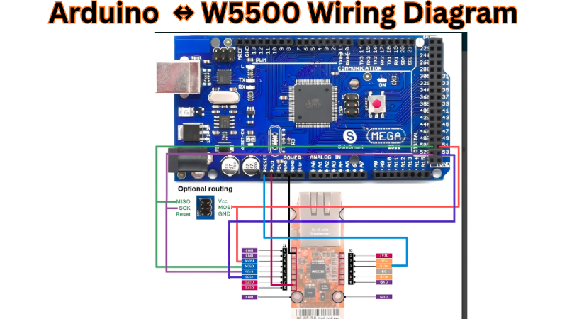
Hardware Wiring — Arduino Uno & W5500
The most critical constraint: the W5500 operates at 3.3V with 5V I/O signal tolerance on its SPI and digital pins. This means the W5500 VCC supply must be 3.3V — use an LDO regulator (e.g., AMS1117-3.3) if your Arduino board only provides 5V — but you can connect SPI signals directly from a 5V Arduino without level shifting.
Arduino Mega SPI pins: MOSI = 51, MISO = 50, SCK = 52. The SS pin (53) must be kept as OUTPUT even if not used as W5500 CS — failing to do so disables the SPI peripheral.
Arduino Library & HTTP GET Example
The Arduino Ethernet library v2 auto-detects W5100, W5200, and W5500 hardware, and Ethernet.init(pin) allows use of any digital pin for the CS signal. No manual chip selection or registry edits are required — the library reads the VERSIONR register at startup and configures itself accordingly.
Library installation: Arduino IDE → Library Manager → search “Ethernet” → install “Ethernet by Arduino”. Version 2.0.0 or later is required for W5500 support.
Full Arduino sketch — DHCP + HTTP GET:
#include <SPI.h>

#include <Ethernet.h>

// W5500 unique MAC address (change per device)

byte mac[] = { 0x00, 0x08, 0xDC, 0x01, 0x02, 0x03 };

EthernetClient client;

const char server[] = "example.com";

void setup() {

  Serial.begin(115200);

  // Set CS pin BEFORE Ethernet.begin()

  Ethernet.init(10);  // Pin 10 = SCSn on Arduino Uno

  // Acquire IP via DHCP (returns 0 on failure)

  if (Ethernet.begin(mac) == 0) {

    Serial.println("DHCP failed — check cable and W5500 power");

    while (true);

  }

  // Verify hardware detected: W5500 linkStatus

  if (Ethernet.linkStatus() == LinkOFF) {

    Serial.println("No Ethernet link — check RJ45 cable");

  }

  Serial.print("IP address: ");

  Serial.println(Ethernet.localIP());

  delay(1000);  // Allow W5500 to stabilize after DHCP

  // Open TCP connection and send HTTP GET

  if (client.connect(server, 80)) {

    client.println("GET / HTTP/1.1");

    client.print("Host: ");

    client.println(server);

    client.println("Connection: close");

    client.println();

  } else {

    Serial.println("TCP connection failed");

  }

}

void loop() {

  // Stream response bytes to Serial

  while (client.available()) {

    Serial.write(client.read());

  }

  if (!client.connected()) {

    client.stop();

    while (true);  // Halt after single request

  }

}
W5500 with Raspberry Pi Pico & MicroPython
MicroPython’s official network.WIZNET5K driver supports the W5500 on RP2040 boards. The network.WIZNET5K(spi, pin_cs, pin_rst) constructor initialises the W5500 module using the given SPI bus and pins; all objects are initialised by the driver internally.
Firmware requirement: Use the official WIZnet MicroPython build for the W5500-EVB-Pico, available at micropython.org/download/?vendor=Wiznet. The standard Pico firmware does not include the WIZNET5K driver by default.
Pico ↔ W5500 SPI pin mapping (W5500-EVB-Pico default):
Complete MicroPython snippet — DHCP + TCP client:
import network

import socket

import time

from machine import Pin, SPI

# --- W5500 SPI + network init ---

spi = SPI(0, 2_000_000,           # Start at 2 MHz for init stability

          mosi=Pin(19),

          miso=Pin(16),

          sck=Pin(18))

nic = network.WIZNET5K(spi, Pin(17), Pin(20))  # spi, CS, RST

nic.active(True)

nic.ifconfig('dhcp')              # Acquire IP via DHCP

# Wait for DHCP assignment (timeout after 15s)

timeout = 15

while nic.ifconfig()[0] == '0.0.0.0':

    timeout -= 1

    if timeout == 0:

        raise RuntimeError("DHCP timeout — check cable/switch")

    time.sleep(1)

print("IP:", nic.ifconfig()[0])   # Print assigned IP

# --- TCP socket connect and HTTP GET ---

addr = socket.getaddrinfo("example.com", 80)[0][-1]

s = socket.socket()

s.connect(addr)

s.send(b"GET / HTTP/1.1\r\nHost: example.com\r\nConnection: close\r\n\r\n")

# Read and print response

while True:

    data = s.recv(512)

    if not data:

        break

    print(data.decode(), end="")

s.close()
Static IP alternative — replace nic.ifconfig(‘dhcp’) with:
nic.ifconfig(('192.168.1.100', '255.255.255.0', '192.168.1.1', '8.8.8.8'))
Key implementation notes:
- SPI clock can be increased to 40 MHz (40_000_000) after DHCP is confirmed stable. Start at 2 MHz during debugging
- nic.ifconfig()[0] returns ‘0.0.0.0’ while DHCP is pending — always poll for a valid IP before opening sockets
- network.WIZNET5K exposes the standard MicroPython BSD socket API — the same socket.socket(), s.connect(), s.send(), s.recv() calls used for Wi-Fi work identically over W5500 wired Ethernet
- For ESP32 with W5500: use the ESP32-Wiznet-W5500-Micropython library — initialize with machine.SPI on any available SPI bus and assign CS/RST GPIO pins accordingly
MCU Compatibility Quick Reference
W5500 vs W5100 vs W5100S — Technical Comparison
The decision of engineers who are considering a WIZnet Ethernet controller IC for a new project is mostly based on one question: “W5100, W5100S, or W5500?” The decision is based only on the number of sockets required, SPI throughput, PCB footprint, and compatibility of existing firmware. This section is intended to provide a direct, verified comparison of all these ICs, allowing a decision based on facts instead of assumptions.
Two corrections from commonly circulated comparison tables: The W5100S SPI speed is 70 MHz — not 14 MHz (that figure applies to the original W5100 only). The W5100S allows the SPI clock to work at a maximum of 70 MHz. The W5100S will be offered in 48-pin LQFP and QFN packages vs. 80-pin for the W5100. Additionally, it has already been established in Section 2 that the W5500 has a package of LQFP48 and not QFN48. These mistakes are rampant in the documents that have been created and should not appear in published technical materials.
Side-by-Side Specification Table
Key Differences Explained
Socket count is the most consequential difference. The maximum number of connections for both W5100 and W5100 is limited to four sockets. A single application using both MQTT + HTTP server + DNS + SNTP occupies all four of the sockets. The W5500, on the other hand, with a total of eight sockets provides a wider range of possible concurrent protocol stacks. This includes the possibility of adding Modbus/TCP, support for over-the-air (OTA) updates, or monitoring using SNMP without exhausting these sockets.
SPI speed gap is real but context-dependent. The 14 MHz SPI limitation on the original W5100 causes a restriction on the maximum burst TCP payload throughput the original W5100 can support. The W5100S increases the maximum burst TCP payload throughput to 70 MHz, but does not have the W5500’s VDM burst mode, which allows an entire 1460 byte TCP segment to be transmitted using a single SCSn assertion.
Package footprint changed significantly. The original W5100 is housed in an LQFP80 package with a large 10 × 10 mm footprint accounting for low density consumer electronics application PCB area. The W5100S has reduced the PCB footprint to a 48 pin LQFP or QFN with a 7 × 7 mm footprint that is identical to the W5500 making the board-to-board migration from W5100S to W5500 only a schematic edit without a need for layout changes.
Firmware compatibility: W5100 → W5100S is a drop-in. Firmware written for the W5100 is compatible with W5100S hardware without modification, making the W5100S the correct upgrade path for any existing W5100-based product in production. Migrating to W5500 requires rewriting register access code to use the W5500’s BSB-based 3-phase SPI frame format — not a complex change, but not transparent.
Decision Guide — Which IC to Use
Migration Path: W5100 → W5500
Migrating a W5100-based design to W5500 involves three areas of change:
Hardware changes:
- Replace LQFP80 footprint with LQFP48 — requires PCB layout revision
- W5500 requires EXRES1 (12.4 kΩ), TOCAP (4.7 µF), and 1V2O (10 nF) passive components not present on W5100 designs
- Crystal circuit remains identical (25 MHz)
- SPI connections are pin-for-pin compatible in function; only physical pin numbers change
Firmware changes:
- All SPI transactions must be updated to use W5500’s 3-phase frame format (Address + Control + Data with BSB field).
- W5100-style direct 16-bit address writes are not valid on W5500
- Socket register offsets are the same; the BSB field in the control byte is the new element
Library changes (Arduino):
- The W5500 is the exact chip used in the Arduino Ethernet Shield 2 and is natively supported by the built-in Arduino Ethernet library — no custom library needed, unlike the W5100S which requires a modified detection routine
- Change: Ethernet.init(CS_PIN) before Ethernet.begin() — same call works for both W5100 and W5500 in Ethernet v2
W5500 PCB Layout & Hardware Design Guidelines
A correctly functioning W5500 design on a bench will fail in production if the PCB layout violates the physical requirements of the analog PHY section. The majority of hardware failures in W5500 designs are due to the following three layout locations; Power supply decoupling, Crystal circuit and Ethernet magnetics. All three of these locations must follow very specific and non-negotiable layout rules. The following section will describe the required layouts with exact values and references taken from WIZnet Design Guide and Datasheet v1.1.0.
Package correction: The W5500 is housed in an LQFP48 package, not QFN48. There is no exposed thermal pad on the bottom of the package — thermal pad guidelines that appear in other articles are incorrect for the W5500 and apply to different ICs. Decoupling strategy is the primary thermal and noise management tool for this chip.
Power Supply Decoupling
The most common cause of unstable PHY behavior, SPI corruption at high clock rates and sporadic link failure that are challenging to replicate are due to power supply noise. The W5500 has a digital VDD and several analog AVDD pins that power the integrated PHY. These must be decoupled independently and routed with discipline.
Decoupling architecture — three layers:
To minimize power supply noise, place a 0.1 uF bypass capacitor close as possible to each input pin of every power pin. In addition to the bypass capacitor, you will also need to place two bulk capacitors (10 uF and 4.7 uF), and then you can connect power through either a Ferrite Bead or 0 Ohm resistor to provide a filtering function for the power and to reduce noise on the power supply.
Precise decoupling values per supply pin:
The 0.1 µF decoupling capacitors should be placed as close as possible to each pin, one for each. The 1 µF capacitor should be placed on the initial power input line.
AVDD vs VDD routing:
It is recommended to distinguish between AGND and DGND. The analog GND pin and digital GND pin should be maintained in a good path. In practice, this means:
- Route the AVDD trace separately from VDD from the ferrite bead or power plane entry point to each AVDD pin cluster
- Do not share via connections between AVDD and VDD — each should have dedicated via drops to the power plane
- We recommend you not to separate analog and digital GND by a split plane. If there is enough GND space, it is better to integrate them into DGND rather than separate them by beads. A unified, low-impedance GND plane is more effective than a split plane for most W5500 designs
PCB layout priority rules:
- Place decoupling capacitors on the same layer as the W5500 — do not route through vias to a capacitor on the opposite side
- Make sure to use many vias for good GND connectivity across layers. A minimum of two vias for each capacitor GND return path, four or more is better.
- It is recommended that GND copper fill be applied to the interior area of the chip footprint to reduce ground impedance directly under the IC
- RSTn power-on reset: it is safer to attach a 4.7 kΩ pull-up resistor to the RSTn pin and a capacitor of at least 1 µF to GND. In cases where the device operates with power sources like PoE, this is not optional but essential.
Crystal & Clock Circuit
The W5500 PHY requires a stable 25 MHz reference clock. An unstable or noisy clock will produce a PHY that fails to link, links intermittently, or shows elevated error rates under thermal or voltage stress.
Crystal selection:
A 25 MHz crystal or oscillator must be installed. When using a crystal, the load capacitance of the W5500 should be calculated and designed to be 18 pF.
Load capacitor calculation:
The two external load capacitors (C_XI and C_XO) are calculated from the crystal’s specified CL:
$CL = (C_XI × C_XO) / (C_XI + C_XO) + C_stray$
$Where C_stray ≈ 3–5 pF (PCB trace + IC input capacitance)$
$For CL = 18 pF and C_stray = 4 pF:$
$(C × C) / (2C) + 4 = 18$
$C/2 = 14 → C = 28 pF → $ use 27 pF standard value
For a CL = 18 pF crystal with estimated 4 pF stray: use 27 pF ±5% COG/NPO ceramic capacitors on both XI and XO. Do not substitute $X5R/X7R$ — their capacitance varies with voltage and temperature, degrading frequency accuracy.
PCB layout rules for the crystal circuit:
- Place the oscillator as close to the chip as possible. Because it is a very high-frequency clock, route traces on the same layer as the chip without vias.
- Keep all three crystal traces (XI, XO, common GND node) under 5 mm total length
- It is recommended that only one chip be connected to one oscillating element. Never share the 25 MHz crystal between the W5500 and another IC
- Surround the crystal circuit with a continuous GND guard ring connected to the GND plane through multiple vias — this prevents adjacent digital signals from coupling noise into the high-impedance crystal oscillator loop
- Do not route SPI, power, or LED traces beneath or beside the crystal circuit on any PCB layer
External clock option: A 25 MHz CMOS oscillator can be fed directly into pin 30 (XI/CLKIN) if there are concerns about either board size or complexity of the crystal circuit. Apply a 3.3 V single-ended output to the oscillator and leave pin 31 (XO) unconnected and floating. In addition, a 3.3 V clock must be applied to the external clock input. If this method is used, do not connect XO or any other pin on the external clock source to anything else.
RJ45 Magnetics & Ethernet Transformer Circuit
The Ethernet transformer connects the W5500 PHY pins to an RJ45 connector and allows for DC isolation (the IEEE 802.3 standard specifies an isolation requirement of 1500V RMS), common mode noise rejection, and proper impedance matching for these two connections. Although the transformer can be omitted from the design, this will increase the noise susceptibility of the overall design and degrade the performance of the Ethernet device.
W5500 MDI signal mode difference from other PHY chips:
Unlike traditional chips, the W5500 has separate RX and TX port levels. The TX and RX side of the W5500 is driven differently than the majority of chips in that the RX side is current driven and the TX side is voltage driven. To drive the RX side in current mode, the CT (center tap) must connect to GND via a capacitor. When driving the TX side in voltage mode, supply power to the CT.
The above distinction also governs how the transformer center tap connections are later made, which is something that the majority of W5500 reference designs from other WIZnet based designs do not show properly.
Two transformer circuit configurations:
Option A — Separate RJ45 + external transformer:
Use an external 10/100 Ethernet transformer (e.g., Würth 749010014, Bothhand BH-MDT-1002NL) with a separate RJ45 connector.
W5500 TXP/TXN → 49.9 Ω series resistors → Transformer TX winding → RJ45 TD+ / TD−
W5500 RXP/RXN → Transformer RX winding → RJ45 RD+ / RD−
TX center tap (TCT): Connect to 3.3V through 49.9 Ω (Voltage Mode termination)
RX center tap (RCT): Connect to GND through 0.1 µF capacitor (Current Mode isolation)
Option B — Integrated RJ45 + magnetics module (recommended for new designs):
The circuit may change depending on the internal circuit configuration of the Ethernet socket. Make sure to refer to the datasheet and design the circuit appropriately. Modules like the HR911105A integrate the transformer, common-mode choke, and LED indicators in a single package:
W5500 TXP/TXN → 49.9 Ω series resistors → HR911105A TX pins
W5500 RXP/RXN → 0.1 µF capacitors → HR911105A RX pins
HR911105A TCT → 49.9 Ω → 3.3V
HR911105A RCT → 0.1 µF → GND
If the RJ45 connector has RCT and TCT tied together internally, it is only necessary to install a capacitor on the RX line. Always verify the specific RJ45 module datasheet — this differs between manufacturers.
Isolation zone layout rule:
A block diagram should show how the RJ45 and PHY device connect, focusing on an isolation region and the ground (GND) connections. On the printed circuit board (PCB), a physical isolation boundary should be shown between the transformer secondary side (RJ45 side) and the transformer primary side (W5500 side). There should be no traces, copper pours, or GND fills that cross this boundary, except for the 1 nF/200 V chassis coupling capacitor. This maintains the 1500 V isolation specified by IEEE 802.3.
MDI differential trace routing:
- Route TXP/TXN and RXP/RXN as 100 Ω differential pairs
- Match trace lengths within ±0.5 mm for each differential pair
- Keep differential pair traces away from all digital signals, SPI lines, and power traces
- Do not use right-angle corners on differential pair routing — use 45° bends or arcs
Common PCB Design Mistakes & How to Avoid Them
Troubleshooting & Common Issues
SPI Communication Checklist
Before attempting any network connection, always verify the SPI communication is working correctly by reading the VERSIONR register — it must return 0x04. If it does not, every subsequent register read and write is meaningless.
Systematic first-contact debug procedure:
// Step 1 — verify power

// Measure pin 28 (VDD): must be 3.3V ± 5%

// Measure pin 4 (AVDD): must be 3.3V ± 5%

// Step 2 — release reset and wait

GPIO_SetPin(RST_PIN);   // RSTn = HIGH

delay_ms(50);

// Step 3 — read VERSIONR

uint8_t ver = w5500_read_byte(0x0039, 0x00);  // BSB=Common, RWB=Read

// Expected: 0x04

// Got 0xFF → SPI hardware issue

// Got 0x00 → MOSI/MISO swapped or Mode mismatch

// Got 0x04 → SPI is working — proceed to network config
No Ethernet Link
Check PHY LINK — bit 0 of PHYCFGR register at address 0x002E — before attempting any socket operation. PHYCFGR_LNK_ON is defined as bit 0 = 1 (link established); PHYCFGR_LNK_OFF is bit 0 = 0 (no link).
uint8_t phycfgr = w5500_read_byte(0x002E, 0x00);

// Bit 0 = LNK: 1 = link up, 0 = no link

// Bit 1 = SPD: 1 = 100 Mbps, 0 = 10 Mbps

// Bit 2 = DPX: 1 = full duplex, 0 = half duplex

if (phycfgr & 0x01) {

    // Link established — proceed

} else {

    // No link — use checklist below

}
No-link hardware diagnostic sequence:
Most common cause of no-link in new designs: The differential pairs for TX and RX were swapped at the transformer. The pin layout of your RJ45/Transformer Module must be verified and compared against the relevant W5500 pin numbers for TXP and TXN. The second most frequent cause of a problem is having a missing EXRES1 or using the wrong value resistor because the value of the EXRES1 should be 12.4 kΩ ±1%.
DHCP & IP Configuration Failures
The W5500 contains no on-chip DHCP client. DHCP must be implemented entirely in host firmware using a UDP socket. If you are using the Arduino Ethernet library, it calls Ethernet.begin(mac) which runs a software DHCP client internally — the W5500 itself is transparent to this process.
Correct static IP initialization sequence:
uint8_t gw[4]  = {192, 168, 1, 1};    // Gateway

uint8_t sn[4]  = {255, 255, 255, 0};  // Subnet mask

uint8_t ip[4]  = {192, 168, 1, 100};  // Device IP

uint8_t mac[6] = {0x00, 0x08, 0xDC, 0x01, 0x02, 0x03}; // Unique MAC

// Control byte for Common Register write: BSB=00000, RWB=1, OM=00 → 0x04

w5500_write_burst(0x0009, 0x04, mac, 6);  // SHAR

w5500_write_burst(0x0001, 0x04, gw,  4);  // GAR

w5500_write_burst(0x0005, 0x04, sn,  4);  // SUBR

w5500_write_burst(0x000F, 0x04, ip,  4);  // SIPR

// Only open sockets AFTER all network config is written
W5500 vs Alternatives — Market Context
Comparison Table
When Each IC Is the Right Choice
The W5500 is the best choice for any new design that needs multiple connections at once, an industrial operating range, or least intervention of the host MCU for networking. This device is WIZnet’s current production recommendation and is the most widely supported IC for Arduino, MicroPython, and C programming.
ENC28J60
ENC28J60 may be used if the only major factor dictating your decision is how much you can save on the cost of the ENC28J60, and if the host’s MCU has enough spare capacity for processing power and RAM to accommodate a software TCPIP stack ( lwIP / UIPEthernet ). Choosing the ENC28J60 is also not recommended. It is limited to 10 Mbps, has a history of instability, and should not be used in any new designs using BSP32 ( ESP32 ) microcontrollers. The ENC28J60 can operate between 0°C and 70°C, which also excludes it from usage within industrial applications.
LAN8720A
LAN8720A should be selected when the host’s MCU has an integrated Ethernet MAC with an RMII interface (typically found within STM32F4/F7/H7 series micros, and variants of ESP32). When using ESP32, the built-in MCU MAC will communicate directly to the LAN8720A via the RMII interface using the TCPIP stack ( lwIP ) built into the MCU, producing much greater throughput than using an external controller, but requires additional clock cycles consumed within the operation of the protocol processing functions on the MCU.
W6100
W6100 should be considered if you have stringent requirements to use both IPv6 and IPv4 within your network. In addition, the W6100 has has both IPv4 and IPv6 capabilities, for both dual-speed 10 / 100 Ethernet communications and a hard-wired stack comm architecture similar to the W5500 Ethernet controller, providing a good upgrade path for W5500 designs that may need to add IPv6 capability without the need to change their code base.
Conclusion
The W5500 is a well-established and well-supported hardwired TCP/IP solution that remains the only viable choice for the vast majority of new IoT and industrial design projects. The eight-socket design, 80 MHz SPI bus with burst mode support, 32 KB buffer memory, and -40°C to 85°C operating temperature range make the W5500 suitable for a wide range of applications from a single sensor node using MQTT to a multi-protocol industrial gateway that supports simultaneous use of MQTT, Modbus/TCP, HTTP, DNS, and SNTP.
Decision matrix for final IC selection:
The architecture of W5500, including pinout, SPI protocol, register map, PCB layout, and IoT integration, represents a complete understanding of implementation that is required for taking a product from schematic capture through firmware development into production. The referenced specifications are all based on the WIZnet W5500 Datasheet v1.1.0, ioLibrary_Driver source, and application notes provided by WIZnet.
Frequently Asked Questions
The W5500 supports UDP on its eight sockets (including multicast and broadcast), but since it does not support IP fragmentation, the UDP payload must be 1472 bytes or less.
The W5500 has no built-in TLS support, so encryption must be handled in the host MCU using libraries like mbedTLS or wolfSSL, requiring about 50 kB SRAM.
The W5500 supports a 10/100 Mbps PHY, but actual TCP throughput is typically 15–25 Mbps and depends mainly on SPI speed and buffer handling rather than the PHY itself.
The W5500 runs on 3.3V power but tolerates 5V logic on SPI pins, though its VCC must never exceed 3.3V.
COMMENTS