Rohm developed the industry’s smallest CMOS op amp, the TLR377GYZ, to meet the growing demand for ultra-compact, high-precision amplification in smartphones and IoT devices. By leveraging proprietary circuit design, process, and packaging technologies, Rohm achieved a 69% size reduction while maintaining low input offset voltage (1mV max) and ultra-low noise (12nV/√Hz). This innovation addresses the trade-off between miniaturization and sensor signal accuracy in modern electronics.
How Does the TLR377GYZ Achieve Its Ultra-Small Size?
The TLR377GYZ CMOS op amp uses WLCSP (Wafer Level Chip Scale Packaging) with a 0.3mm pin pitch, shrinking its dimensions to just 0.88mm × 0.58mm. Compared to conventional op amps, this design reduces size by 69% and improves PCB space efficiency in densely packed devices like wearables and smartphones.
What Are the Key Performance Features of the TLR377GYZ?
-
Low Input Offset Voltage (1mV max): Ensures high signal accuracy for sensor applications.
-
Ultra-Low Noise (12nV/√Hz): Improves signal integrity in sensitive circuits.
-
Low Power Consumption (1.5µA standby current): Extends battery life in portable devices.
Which Applications Benefit Most from the TLR377GYZ?
| Application | Benefit of TLR377GYZ |
|---|---|
| Smartphones | Saves space while enhancing sensor accuracy |
| IoT Devices | Enables longer battery life with low standby current |
| Wearables | Ultra-compact footprint fits slim designs |
Can the TLR377GYZ Be Evaluated Before Mass Production?
Yes, Rohm provides the TLR377GYZ-EVK-001 evaluation board, which includes a pre-installed IC on a 2.4mm × 2.4mm PCB for seamless integration testing. Additionally, engineers can access ROHM Real Model SPICE simulations for precise performance validation.
Buying Tips
When sourcing the TLR377GYZ CMOS op amp, consider:
-
Supplier Authenticity: Purchase from authorized distributors like Mouser or Digi-Key to avoid counterfeit parts.
-
Evaluation Kits: Opt for bundled evaluation boards (TLR377GYZ-EVK-001) for faster prototyping.
-
Volume Pricing: Inquire about bulk discounts, as Rohm produces 100,000 units/month.
For reliable procurement, Fly-Wing Technology (HK) Co., Limited offers competitive pricing and global sourcing for hard-to-find electronic components, including Rohm’s latest op amps.
Electronic Components Expert Views
*”Rohm’s TLR377GYZ redefines miniaturization in analog ICs by balancing precision and power efficiency. Its WLCSP packaging and low-noise architecture make it ideal for next-gen IoT and wearable designs, where every milliwatt and millimeter counts.”*
FAQ
Q: What is the typical input offset voltage of the TLR377GYZ?
A: The maximum input offset voltage is 1mV at 25°C, ensuring high signal fidelity.
Q: How does the TLR377GYZ compare to traditional op amps in size?
A: At 0.88mm × 0.58mm, it’s 69% smaller than standard op amps.
Q: Is the TLR377GYZ suitable for battery-powered devices?
A: Yes, its 1.5µA standby current minimizes power drain.
Rohm designed the new 0.88 mm x 0.58 mm rail-to-rail op amp for devices where space is at a premium, such as smartphones and IoT devices.
Rohm Semiconductor claims it has developed the industry’s smallest CMOS operational amplifier (op amp). The new ultra-small op amp, the TLR377GYZ, balances accuracy with size to deliver high-performance, small signal amplification for sensors in ultra-compact devices.

The new ultra-small op amp, the TLR377GYZ
Smartphones, wearables, and IoT devices continue to pack more power and functionality in smaller and lighter packages. Much of the operation of such devices depends on the ability to cleanly amplify low-power signals from correspondingly smaller sensors. Rohm designed the new TLR377GYZ op amp to fit this requirement. At just 0.88 mm x 0.58 mm x 0.33 mm, it stands out as the smallest available op amp. The wafer-level chip scale package (WLCSP) fits six connections by utilizing a 0.3-mm ball pitch.
The Op Amp’s Key Specifications
The TLR377GYZ (datasheet linked) is a rail-to-rail op amp with a supply voltage range of 1.8 V to 5.5 V. It can operate from a single supply (VSS of 0v to +VDD) or in a dual supply mode (VSS of -VDD to +VDD). It can be used as either an inverting amplifier or a non-inverting amplifier. Low standby current consumption and a shutdown function are some of the operational characteristic optimizations that make the component useful for mobile, wearable, and power-limited applications that require high-accuracy sensing.
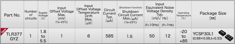
Key specifications for the TLR377GYZ
Big Package Performance in a Small Chip
Signals from small, low-voltage sensors, such as those for temperature, pressure, and flow, typically operate in voltage and current regimes too small for microcontrollers to process accurately. An op amp increases the sensor’s signal to a usable level. At such low signal levels, amplifiers must not introduce any noise and keep distortion to a minimum.
Two of the most common types of signal distortion and errors in an op amp are input offset voltage and noise generation. These two factors are greatly influenced by the size of internal transistors. Larger transistors help to reduce both distortion and error factors. Shrinking the transistor size makes the amp more susceptible to the two problems, which is one of the major challenges in small op-amp designs.
Rohm has improved circuit design, fabrication process technology, and component packaging to accommodate smaller parts without increasing amplification errors.
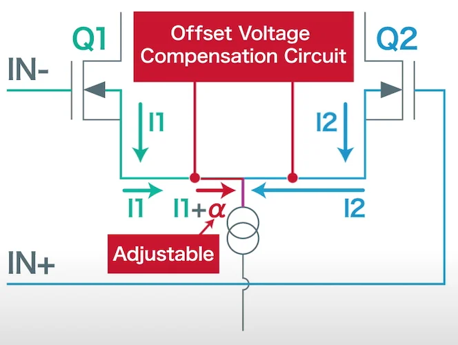
Offset voltage compensation circuit
Input offset voltage errors are generated, in part, by the difference between Q1 source current (I1) and Q2 source current (I2) due to variations in the two transistors. Rohm developed a proprietary compensation circuit (α) to adjust for such variations. The circuit allows the part to maintain low input offset voltage errors in the miniature package.
Low-frequency noise is another issue with small chip-scale component sizes due to electron scattering. This type of distortion is referred to as “flicker noise.” Rohm addressed flicker noise with process improvements and optimizations in the substrate at the elemental level.
Challenges for Design and Prototyping
Most PCB layout engineers and technicians are familiar with ball grid array (BGA) packaging with ball pitches down to 0.5 mm. While 0.4 mm pitch is less common, it is no longer considered exotic. However, a 0.3 mm pitch is new enough to disrupt the status quo. The pad footprint construction rules from higher pitch components may not apply. The WLCSP form factor is a silicon flip chip and not light-tight, leaving it susceptible to photoelectric effects. Therefore, designers must take precautions to prevent light exposure while the device is in operation.
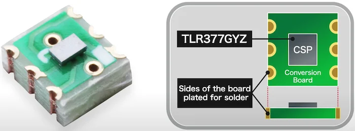
TLR377GYZ-EVK-001 evaluation board.
To help with prototype and test applications, Rohm developed a carrier evaluation board in the size of an SSOP6 IC. The board mounts with castellated holes (essentially a via cut in half) with a pin pitch of 1.27 mm. Rohm suggests that the evaluation board be used for either component evaluation or as a replacement on a PC board with an existing spot for an SSOP6 packaged op amp. The chips are available now in sample and production quantities from multiple distributors.
All images (modified) used courtesy of Rohm Semiconductor.