Introduction
Most sensors, such as temperature, pressure, motion, and proximity sensors, provide very low output voltage, mostly in the range of millivolts (mV) or microvolts (μV) at the output. Upon interfacing with the microcontroller, it uses an analog-to-digital converter (ADC) to read the sensor output. If the sensor output is below the ADC resolution. It does not detect the output of the sensor; therefore, a specialized device is use to eliminate the noise from the sensor output signal and amplify it such that it can be recognize by the microcontroller ADC.
One of such most popular operational amplifiers is LM741. The LM741 IC consists of a single op-amp with inverting, non-inverting inputs, and one output. Due to its high gain, wide operating voltage, input/output overvoltage protection, with no oscillations, the LM741 operational amplifier is widely use for amplification, signal conditioning, active filters, and summing amplifiers.
LM741 as an Operational Amplifier
An operational amplifier, such as LM741, is a voltage-control device that amplifies weak and low-voltage signals. Originally manufactured and introduced by Fairchild Semiconductor in 1968, it gain popularity due to its high gain, overvoltage protection, and wide supply operating range.
This operational amplifier IC consists of 8 PINs that include inverting, non-inverting inputs, and an output. The output gain of the LM741 IC can be found using the external resistors. Typically, LM741 is capable of amplifying the small input signal up to 200,000 times. The op amp has a supply voltage range of ±5V to ±18V, high input impedance up to 2MHz, short circuit protection, and the ability to efficiently handle negative feedback. Therefore, the LM741 operational amplifier is one of the most famous and widely used op amps in analog electronic circuits. Because of its ease of use, simple plug-and-play, and reliability, makes it the first choice of students, hobbyists, and beginner electronic engineers.
LM741 as an Inverting Amplifier
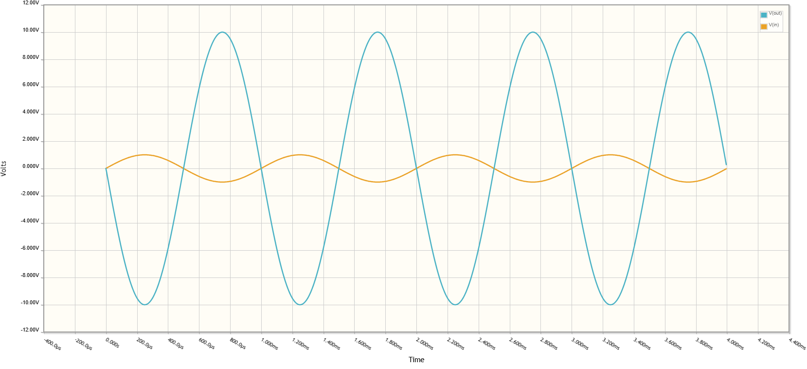
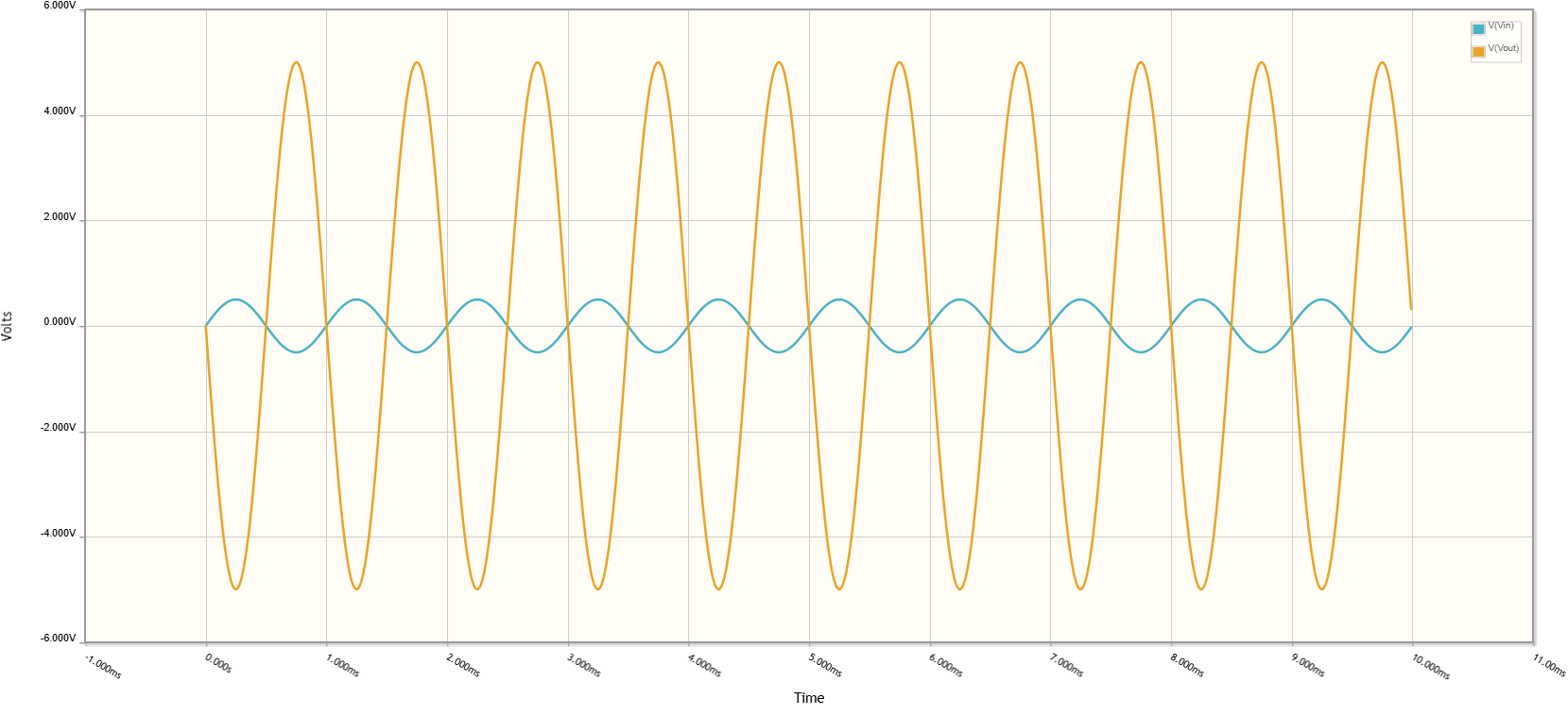
In an inverting amplifier, the signal is fed into the inverting terminal of the op amp. Connect the non inverting terminal of LM741 with GND. The feedback is given at the inverting input from the output of LM741. The output gain is determine using the external resistors R1 and R2.
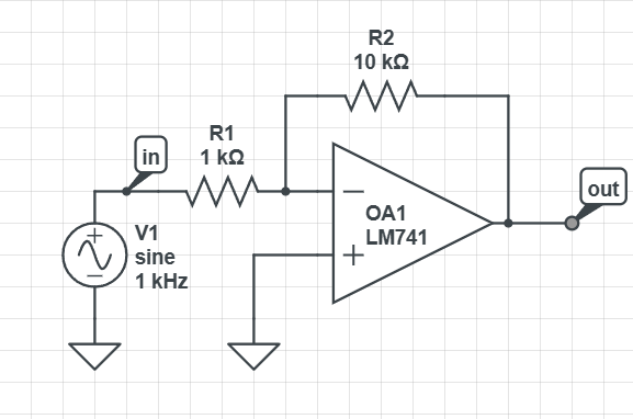
For example, the feedback resistor R2 has a value of 10KΩ, and the input resistor R1 has a value of 1KΩ. The output gain of such an operational amplifier is;
\[
A_V = -\frac{R_f}{R_i}
\]
\[
A_V = -10
\]
so, the output voltage is;
\[
V_{out} = A_V \times V_{in}
\]
\[
V_{out} = -10 \times 1V
\]
\[
V_{out} = -10V
\]
LM741 as a Differentiator Amplifier
The LM741 is also use to perform the mathematical operation of differentiation. In the inverting amplifier configuration, a capacitor is use at the inverting input and a resistor in the feedback from the output of the LM741.
Working Operation:
Connect the capacitor at the input and inverting terminal of the LM741 for differentiation, and a place the resistor in the feedback loop. The impedance of the capacitor is;
\[
X_c = \frac{1}{2 \pi f C}
\]
he voltage gain of the differentiator circuit with the LM741 is
\[
A_v = \frac{R_f}{X_c}
\]
Therefore, ideally at low frequencies (suppose f=0)
At Low Frequencies – Low Output Gain
| Xc | Av |
|---|---|
| Xc = 1/(2π f C) = 1/0 = ∞ | Av = Rf/Xc = Rf/∞ = 0 (Low Gain) |
However, at high frequencies (suppose f=∞)
At High Frequencies – High Output Gain
| Xc | Av |
|---|---|
| Xc = 1/(2π f C) = 1/∞ = 0 | Av = Rf/Xc = Rf/0 = ∞ (High Gain) |
So, in the LM741 differentiator circuit, we conclude that at low frequencies, the reactance of the capacitor will become high, resulting in low gain and low output voltage. However, at high frequencies, the reactance of the capacitor will become low, resulting in high gain and high output voltage.
From the LM741 differentiator circuit, as shown in the LM741 schematic in Proteus, the node voltage of the op amp at the inverting terminal is zero due to the high input impedance of LM741 operational amplifier. Therefore, the input current will flow from the capacitor to the feedback resistor of the operational amplifier, which states;
\[
I = \frac{-V_{out}}{R_1}
\]
The charge through the capacitor is equal to
\[
Q = C \times V_{in}
\]
The rate of change of charge thus;
\[
\frac{dQ}{dt} = C \frac{V_{in}(t)}{dt}
\]
\[
\text{Where } \frac{dQ}{dt} = I
\]
\[
\therefore \quad \frac{-V_{out}}{R} = C \frac{V_{in}(t)}{dt}
\]
\[
V_{out} = -RC \frac{dV_{in}(t)}{dt}
\]

This simply indicates that the output voltage is RC times constant and the derivative of the input voltage. The negative signs show that the output is a 180 ° phase shift because the LM741 is use in an inverting configuration.
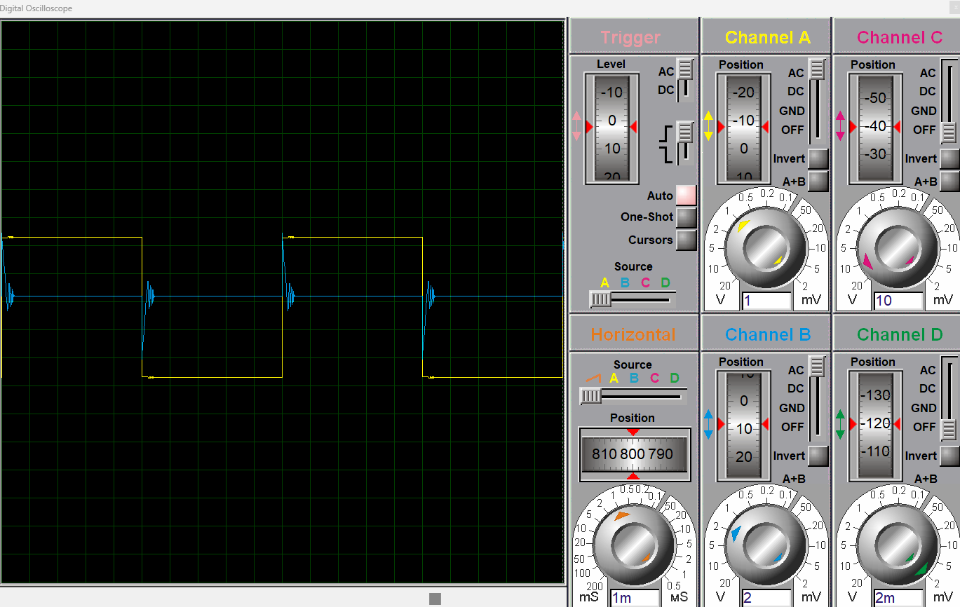
So, when the square wave is given at the input terminal of the LM741 differentiator circuit, the output is the derivative of the square wave input. The derivative of the square wave is spikes, as shown in the output waveform of the differentiator circuit.
LM741 PIN Configuration
The LM741 operational amplifier consists of 8 PINS and comes in many packages such as DIP (Dual In-line Package), TO-99, and CDIP (Ceramic-DIP). This operational amplifier has a single op-amp circuit with inverting and non-inverting inputs and a single output. Due to its simplicity and ease of use, it is among the most widely use and sold operational amplifiers across the globe.

The 8 PINS of LM741 each have a distinct function. Always refer LM741 datasheet for the exact pinout for different variants.
LM741 Operational Amplifier Pin Configuration
| Pin Number | Pin Name | Function |
|---|---|---|
| 1 | Offset Null | This pin eliminates the offset voltage and balances the input voltages |
| 2 | Inverting Input | Inverting input signal |
| 3 | Non-inverting Input | Non-inverting input signal |
| 4 | V- | Negative supply voltage of the IC |
| 5 | Offset Null | This pin eliminates the offset voltage and balances the input voltages |
| 6 | Output | This is the output PIN of LM741 |
| 7 | V+ | Positive supply voltage of the IC |
| 8 | NC | This is an NC (not connected) PIN, and should be left floating |

Internal Block Diagram and Working Principle
The LM741 operational amplifier is one of the most popular amplifiers that are commonly use in analog electronics. Understanding its internal circuit helps the engineers troubleshoot and diagnose the circuit faults. By breaking down the LM741 internal circuit, we can divide the LM741 schematic into three main stages.
Differential amplifier Stage
The first stage of the LM741 internal circuit consists of a differential amplifier circuit. A differential amplifier is the circuit that compares the two inverting and non-inverting inputs and amplifies the difference between the inputs. The differential amplifier is built using the Q1 and Q2 transistors as shown in the schematic. When the input signal is applied at the inverting (-IN) and non-inverting (+IN) terminals, it amplifies the difference between these inputs. The current mirror circuit is built using Q3, Q4, Q5, and Q6 as shown in the circuit schematic rejects the common mode signals. This stage of the LM741 determines the input impedance and common mode rejection ratio (CMRR) of the operational amplifier. In short, this stage will amplify the difference between inputs and reject the noise present in the input signals.

Bias and Gain Stage
This stage consists of the intermediate gain stage, current mirror circuits, and bias generator circuit (Q9, Q10, Q11). The gain stage and current mirror circuit amplify the voltage difference of the input stage. The bias generator ensures a constant reference current for the input and output stages and minimizes any voltage fluctuations. This stage will amplify the signal by 200,000 times in the case of LM741, as per the datasheet.
Output Amplifier Stage
Before the output stage, a level shifter circuit is use in the LM741 internal circuit to shift the DC level of the signal. This is important to ensure that the output is centered at 0V. The difference in signal is amplified, but it cannot drive the load. To do this, an output amplifier stage is built using a class AB push-pull amplifier as shown in the LM741 internal schematic. This stage will ensure to provide low output impedance to drive external loads, and a large output voltage swing.
By understanding the working operation of the internal circuit of LM741, a block diagram can be built that simplifies the working operation.

Electrical Characteristics of LM741
LM741 op amp has some important electrical characteristics which must be consider in the circuit design to efficiently utilize the op-amp capabilities.
LM741 Electrical Characteristics
| Parameter | Value | Function |
|---|---|---|
| Supply Voltage | ±15V | LM741 IC safe operating range |
| Input Impedance | 2 MΩ | High impedance ensures minimum loading of the source |
| Input Offset Voltage | 1–5 mV | Minimum DC input voltage to make the output zero |
| Input Bias Current | 1.5 µA | The small difference between the input bias currents |
| Slew Rate | 0.5 V/µs | Maximum speed of the output voltage |
| Output Voltage Swing | ±14V | The maximum output voltage of LM741 |
| Open Loop Gain | Typically 200,000 | An op-amp’s ability to amplify the input signal |
| Common Mode Rejection Ratio (CMRR) | 95 dB | LM741’s ability to reject the common mode |
These electrical characteristics are important for anyone who is utilizing or interfacing the LM741 in their circuit designs. Always refer datasheet for the exact values of the specific LM741 IC.
Circuit Design and Calculations with LM741 Op Amp
LM741 is the most commonly used operational amplifier, and it is specifically designed for general-purpose applications such as signal amplification, signal conditioning, active filters, and summing amplifiers. The basic circuit design with LM741 requires properly powering up the op amp, identifying the circuit configuration, and then using the external components, such as resistors and capacitors, to properly configure it.
In this section, I will explain simple circuit designs along with their design calculations. Readers can simply design the circuit and use the calculations, and adjust them for their own specific circuits.
Inverting Amplifier
An inverting amplifier is a circuit in which the signal input is given at the inverting terminal (PIN 2) and the non-inverting terminal is connected to GND. The feedback is given to the inverting input from the output terminal (PIN 6) of LM741. When the feedback is given back to the inverting input known as the closed loop gain. This close-loop gain is found using the formula;
\[
\frac{V_{out}}{V_{in}} = -\frac{R_f}{R_1}
\]
\[
A_v = -\frac{R_f}{R_1}
\]
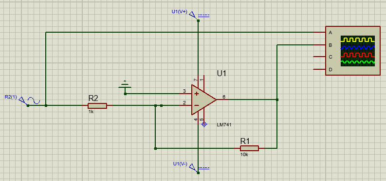
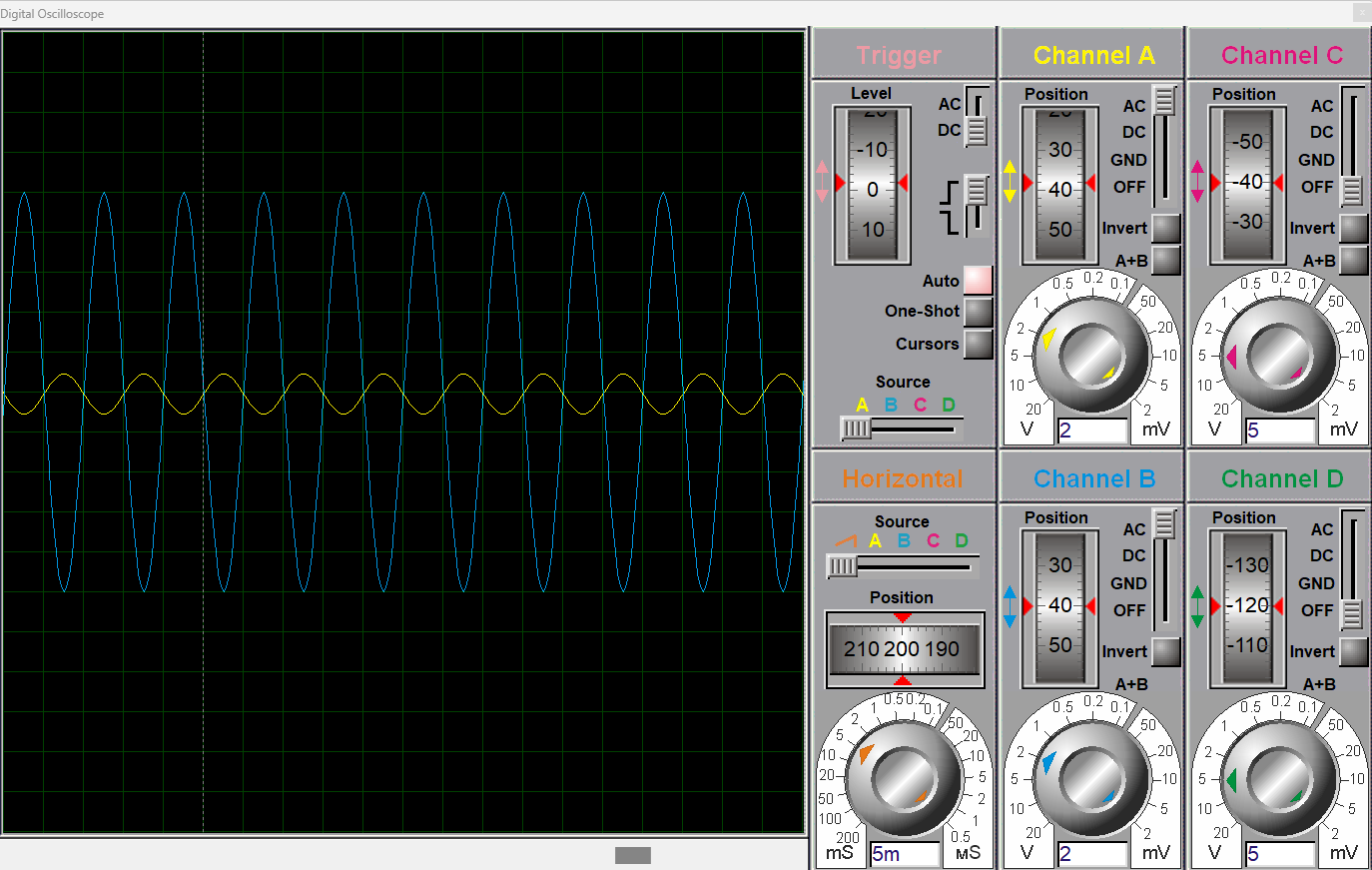
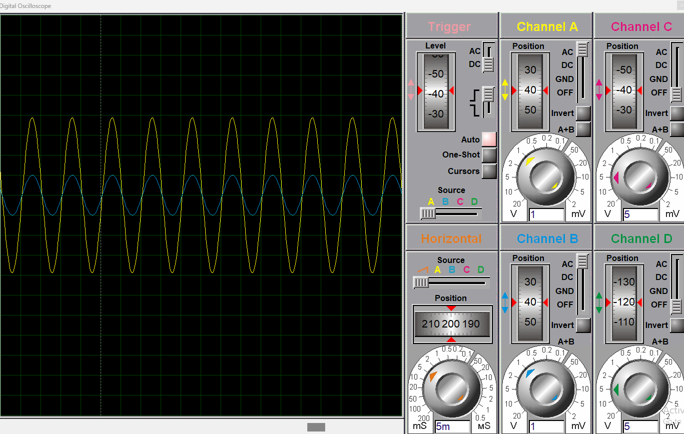
For example, when the feedback resistor value is 10k and R1 is 1k. It will produce a voltage gain of 10 with a 180° phase shift as shown in the output waveform of inverting amplifier circuit.
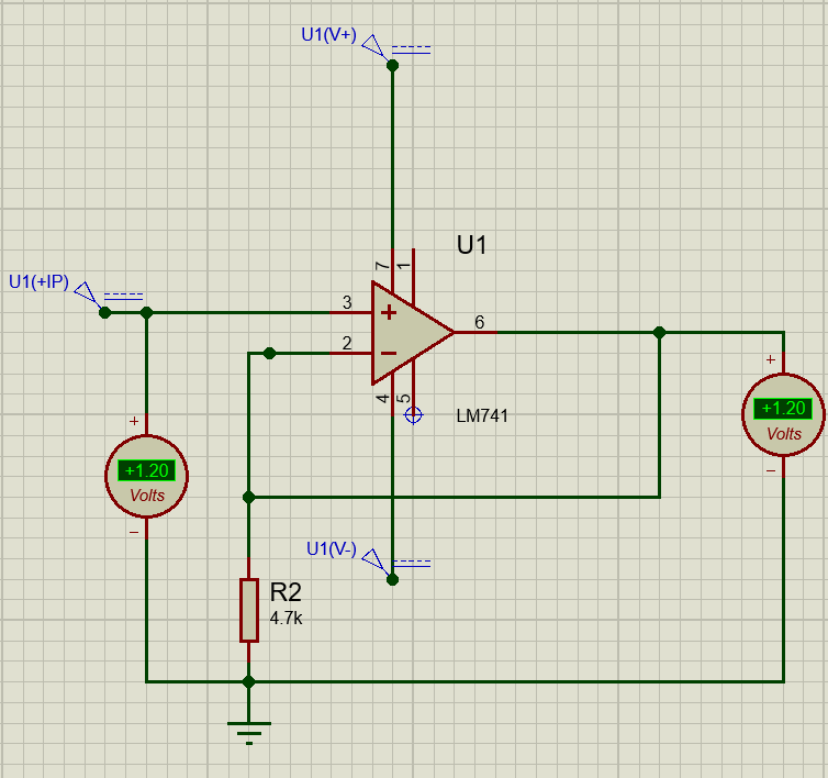
Non-Inverting Amplifier
In a non-inverting amplifier circuit, we apply the input signal to the non-inverting input terminal (PIN 3) of LM741 and connect the inverting terminal (PIN 3 of LM741) with GND. Like for an inverting amplifier, the feedback is given at the inverting terminal of LM741 from the output terminal (PIN 6). The close-loop gain of a non-inverting amplifier is found using the formula;
\[
\frac{V_{out}}{V_{in}} = 1 + \frac{R_f}{R_1}
\]
\[
A_v = 1 + \frac{R_f}{R_1}
\]
For example, when the required output voltage is 13.2 volts for the input signal of 1.2 volts. In the non-inverting configuration, the feedback resistor is set to 47kΩ, and the R1 resistor is set to 4.7kΩ. This will set the voltage gain to 11 and produce the 13.2 volt output as shown in the schematic.
\[
A_v = 1 + \frac{47k}{4.7k}
\]
\[
A_v = 11
\]
Therefore, when the input voltage is 1.2 volts, the LM741 non-inverting amplifier produces a 13.2 Volt output with zero phase shift as shown in the schematic.

Unity Gain Buffer
The LM741 operational amplifier can be configure to act as a unity gain buffer circuit. By directly connecting the output terminal with the input terminal of the operational amplifier. This circuit is also known as the voltage follower.
\[
A_v = 1 + \frac{0}{4.7k}
\]
\[
A_v = 1
\]
When we connect the output terminal of LM741 directly to the inverting terminal. This will create a unity gain or voltage follower circuit with LM741 as shown in the figure.
Common Circuit Applications with LM741
LM741 is a general purpose operational amplifier that is widely use in modern and analog electronics due to its versatility, high gain, cost-effectiveness, and ease of integration into any circuit. In this section, I will use the LM741 operational amplifier in some of the most common applications, such as summing amplifiers, battery charger circuits, and audio amplifier circuits.
Audio Amplifier circuit using LM741
A simple audio amplifier circuit can be built using the LM741 operational amplifier. The LM741 is configure as a non-inverting amplifier. The small voltage AC signal (typically from a microphone or an MP3 player) is given at the input of a non-inverting amplifier. This low audio signal is amplified such that it can be able to drive the audio amplifier.
In the audio amplifier schematic, two low audio signals of 30mV and 1V are applied at the non-inverting input with a single-pole double-throw (SPDT) switch. The different gain levels are set using the feedback resistors, each with a switch. These different gain levels are use for amplifying the audio signal. The different gain stages are shown in the schematic.
\[
A_{v1} = 1 + \frac{10k}{10k} = 2
\]
\[
A_{v2} = 1 + \frac{50k}{10k} = 6
\]
\[
A_{v3} = 1 + \frac{100k}{10k} = 11
\]
\[
A_{v4} = 1 + \frac{220k}{10k} = 23
\]
The input capacitor is use to block the DC content and only allows the AC. Whereas, the output capacitor is use to block the DC content, if any, present in the output signal. However, It must be taken into account that LM741 is not specifically designed for audio amplifiers such as TL072. However, it is still able to drive the low-power applications.

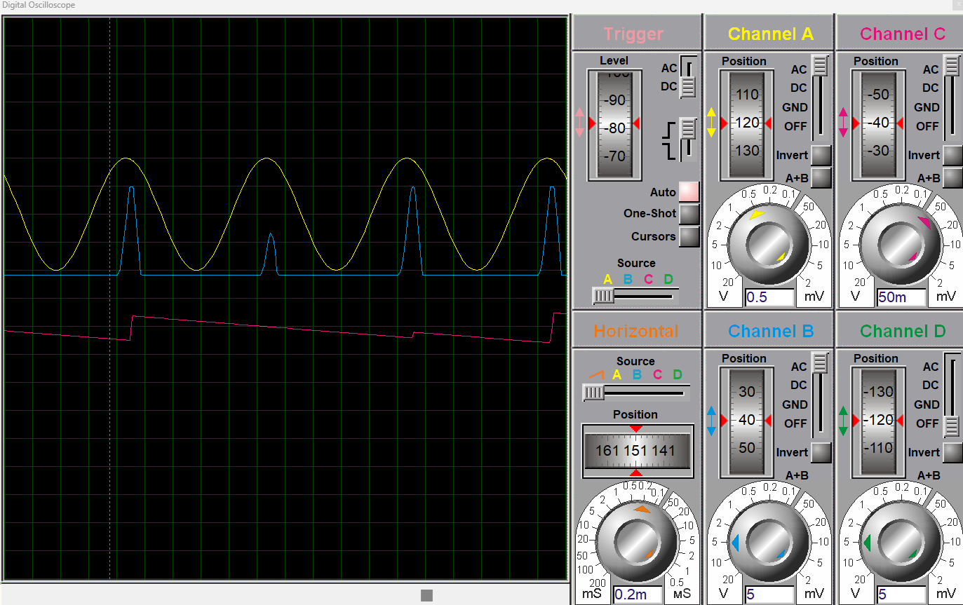
Peak Detector circuit using LM741
Another unique and powerful application of an operational amplifier, such as LM741, is to use it as a peak detector. When the operational amplifier LM741 is use with a diode in a circuit, it can detect the peak of the input voltage signal. This simple application is use in radio and RF circuits to detect the transients in the input signals.
To build a peak detector, the LM741 op amp is configure in the non-inverting amplifier configuration. That means the input signal is being applied at the non-inverting terminal. The diode is place at the output terminal of LM741. The output of the diode is fed back to the inverting terminal to make a unity feedback configuration.
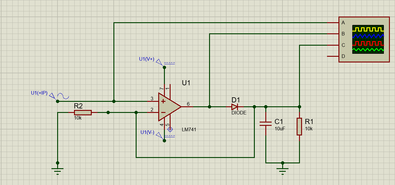
As we apply the input AC signal at the input of LM741, it produces the same signal at the output due to the unity feedback. As the input signal rises above 0.7 forward voltage drop of the diode, it becomes forward biased, and the capacitor will start charging. When the input voltage reaches the highest peak, the capacitor holds the peak because it blocks the reverse current, as shown in the output waveform of the peak detector circuit.
As the voltage at the input falls, the voltage at the anode terminal of the diode becomes less than the cathode terminal. This causes the diode in a reverse-biased condition and blocks the input signal. The capacitor will start discharging through the load resistor. Once the capacitor is below the input
signal, the diode becomes again forward biased
Limitations and Advantages of LM741
The versatile LM741 operational amplifier is most commonly use in both small industries and educational setups. However, there are certain limitations of LM741 which we discuss in this section. To know the limitations of any integrated chip is essential for engineers, as it allows them to make informed decisions in their circuit designs.

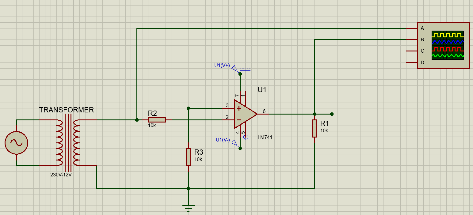
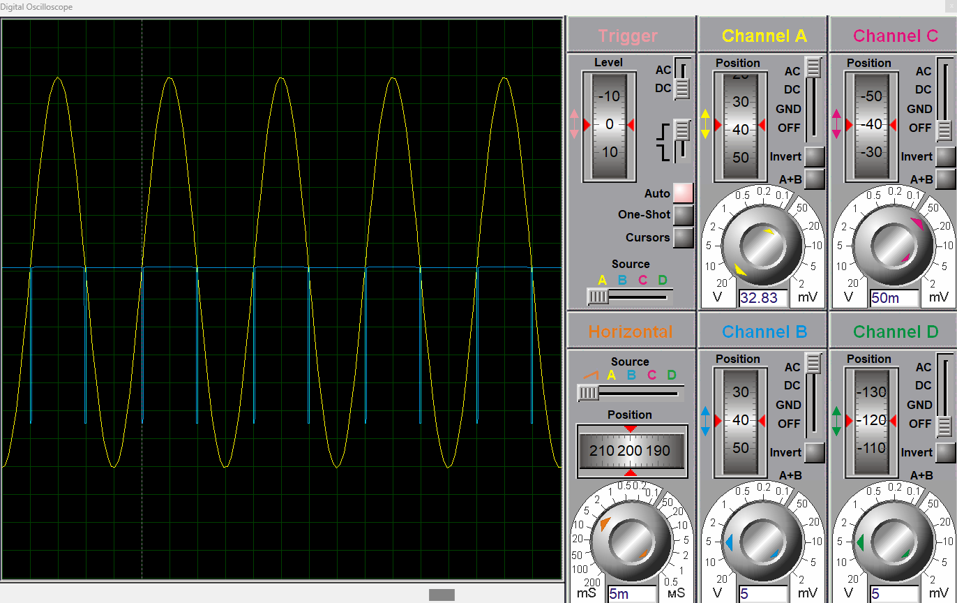
Simulation Results: Zero Crossing Detector with LM741
Zero crossing detector (ZCD) is a simple circuit but is extensively use in digital signal processing, phase lock loops, AC control circuits, and frequency counters. It is a simple circuit that detect the input signal whenever it crossing the zero voltage level.
It can be easily built using the LM741 operational amplifier. Apply the input signal at the inverting terminal of LM741 OP amp. Connect the non inverting terminal with ground to make the zero voltage reference as shown in the circuit schematic. The operational amplifier in this application is configure in open loop configuration.
When the AC input sine wave is in positive half cycle and greater than zero reference volts. The LM741 goes to the negative saturation level (-VCC) as shown in the output waveform.
inverting input > non-inverting input → Output = Negative Saturation (-12V)
When the AC input sine wave is in negative half cycle and less than the zero reference volts. The LM741 goes to the positive saturation level (+VCC) as shown in the output waveform.
inverting input < non-inverting input → Output = Positive Saturation (+12V)
However, when the input sine wave is at the zero volt, and equal to the zero volt reference. It switches the output state from +VCC to -VCC or vice versa.
Conclusion
In conclusion, LM741 is extensively use in analog electronic circuits due to its simple design, ease of use, and high gain. Therefore, it is a popular choice for teachers, students, hobbyists, and early-career professionals. Understanding the circuit design, its working operation helps the designers to utilize them in their desired electronic applications. It is a perfect choice for low-frequency applications and is only use for general-purpose applications such as active filters, oscillators, peak detectors, and zero crossing detectors. For high-speed applications, LM324 and TL072 can be use as an alternative to this op amp.

Frequently Asked Questions (FAQ)
Q1. Why is LM741 popular?
LM741 is a versatile operational amplifier that is easy to use and cost-effective, making it perfect for students, teachers, and early-career professionals.
Q2. What are the limitations of the LM741 op amp?
Low output drive current (20mA), limited bandwidth, and slow slew rate are some of the limitations of the LM741 operational amplifier.
Q3. What is the alternative op amp I can use instead of LM741?
You can use the LM358 op amp, NE5532, and LM324 operational amplifier as an alternative to the LM741.
Q4. Can we use LM741 in audio amplifier circuits?
Yes, but only for low-frequency audio applications. For high audio applications, you can use TL072.
Q5. What is the difference between LM741 and LM358?
LM741 is a general-purpose and low-frequency application amplifier. The LM358 is a modern low-power and dual op amp that has better performance compared to the LM741.