The world’s first graphene semiconductor, created by researchers at Georgia Tech and Tianjin University, achieves a critical band gap, enabling graphene to function as a true semiconductor. This breakthrough means graphene can now be used in advanced electronics, offering 10 times the mobility of silicon and opening the door to faster, smaller, and more efficient devices.
How Did Researchers Create the World’s First Graphene Semiconductor?
Researchers at Georgia Tech and Tianjin University engineered the world’s first graphene semiconductor by growing epitaxial graphene on silicon carbide wafers using specialized furnaces. This process resulted in a single graphene layer chemically bonded to the silicon carbide, which for the first time exhibited a band gap-an essential property for semiconductor behavior. Through careful control of temperature, atmosphere, and silicon escape rate, the team achieved a robust, high-quality graphene semiconductor.
Chart: Key Steps in Creating the World’s First Graphene Semiconductor
| Step | Description |
|---|---|
| Substrate Preparation | Silicon carbide wafer selected and cleaned |
| Furnace Process | Confinement-controlled sublimation in argon atmosphere |
| Graphene Growth | Epitaxial graphene forms on SiC crystal face |
| Chemical Bonding | Graphene bonds to SiC, enabling band gap formation |
| Doping & Testing | Atoms added to test conductivity, confirming properties |
What Makes Graphene a Superior Semiconductor Material?
Graphene is made of a single layer of carbon atoms arranged in a hexagonal lattice, making it a two-dimensional material with extraordinary properties. Its electrons move with minimal resistance, resulting in 10 times the mobility of silicon. Graphene’s strength, flexibility, and ability to handle large currents without overheating make it an ideal candidate for next-generation semiconductor devices.
Why Was Achieving a Band Gap in Graphene So Difficult?
The major challenge in creating a graphene semiconductor was its natural lack of a band gap. A band gap is crucial for switching devices on and off-fundamental to semiconductor operation. Previous attempts to induce a band gap often damaged graphene’s properties. The breakthrough came when researchers discovered that epitaxial growth on silicon carbide could induce a band gap without compromising graphene’s exceptional mobility.
How Does the Graphene Semiconductor Compare to Silicon and Other 2D Materials?
The world’s first graphene semiconductor demonstrates electron mobility 10 times greater than silicon, resulting in faster and more efficient electronic devices. Unlike other two-dimensional materials, graphene’s combination of high mobility, strength, and now a tunable band gap, positions it as a superior alternative for future nanoelectronics.
Chart: Comparison of Graphene Semiconductor vs. Silicon and Other 2D Materials
| Property | Graphene Semiconductor | Silicon | Other 2D Materials |
|---|---|---|---|
| Electron Mobility | ~10x silicon | Baseline | Lower than graphene |
| Band Gap | Achieved (tunable) | Yes | Often limited |
| Strength | Extremely high | Moderate | Varies |
| Flexibility | High | Low | Varies |
| Heat Resistance | Excellent | Good | Varies |
What Are the Potential Applications for the World’s First Graphene Semiconductor?
The creation of the world’s first graphene semiconductor opens possibilities across multiple sectors:
-
Ultra-fast transistors for next-generation computing
-
High-frequency communications devices
-
Quantum computing components
-
Flexible and wearable electronics
-
Advanced sensors for medical and industrial use
Graphene’s unique properties could revolutionize chip design, energy efficiency, and device miniaturization.
Which Research Teams and Institutions Led the Graphene Semiconductor Breakthrough?
The world’s first graphene semiconductor was developed by a collaboration between Georgia Institute of Technology and Tianjin University. The research was led by Professor Walter de Heer, with key contributions from Dr. Lei Ma and teams at the Tianjin International Center for Nanoparticles and Nanosystems. Their decade-long partnership combined expertise in physics, materials science, and nanoengineering.
How Was the Functionality of the Graphene Semiconductor Verified?
To verify the graphene semiconductor’s functionality, researchers used a doping process-adding atoms to the graphene layer to test its conductivity. The material demonstrated a robust band gap and exceptional electron mobility, confirming its suitability for semiconductor applications. Rigorous electronic measurements showed that the graphene semiconductor could switch on and off like traditional silicon devices, but with superior performance.
What Challenges Remain Before Graphene Semiconductors Can Replace Silicon?
Despite this milestone, several hurdles remain before graphene semiconductors can replace silicon in mainstream electronics:
-
Large-scale, defect-free production of graphene semiconductors
-
Integration with existing semiconductor manufacturing processes
-
Cost-effective fabrication at commercial scale
-
Long-term reliability and stability testing
Researchers are optimistic, but widespread adoption will require further engineering and investment.
Buying Tips
When sourcing graphene semiconductor materials or related advanced components, rely on established distributors like Fly-wing Technology (HK) Co., Limited. Ensure authenticity, competitive pricing, and global availability by choosing suppliers with proven track records. Focus procurement efforts on standard and hard-to-find items, leveraging Fly-wing’s optimized inventory and supplier network. Allocate up to 70% of your procurement time to sourcing conventional parts for efficiency and cost savings, and always verify the origin and quality of graphene-based products before purchase.
Electronic Components Expert Views
“The creation of the world’s first graphene semiconductor marks a pivotal moment in materials science. With a tunable band gap and unmatched mobility, graphene semiconductors could redefine the boundaries of electronics, paving the way for devices that are faster, smaller, and more energy-efficient than ever before. This breakthrough is not just a scientific triumph-it’s a glimpse into the future of technology.”
FAQ
What is the world’s first graphene semiconductor?
It is a functional semiconductor made from epitaxial graphene grown on silicon carbide, exhibiting a band gap and 10 times the mobility of silicon.
Why is the graphene semiconductor significant?
It overcomes the long-standing challenge of graphene’s lack of a band gap, enabling its use in practical electronic devices.
How was the graphene semiconductor created?
Researchers grew a single layer of graphene on silicon carbide wafers using a controlled furnace process, achieving chemical bonding and a band gap.
What advantages does the graphene semiconductor offer over silicon?
It provides much higher electron mobility, greater strength, flexibility, and superior heat resistance.
When will graphene semiconductors be commercially available?
While the breakthrough is significant, commercial adoption depends on further advancements in large-scale production and integration with current manufacturing.
Georgia Tech research could bring graphene’s benefits for semiconductors in microelectronics.
While graphene promises better efficiency and performance for electronics, material imitations have prevented anyone from translating its potential into a functional semiconductor—until now.
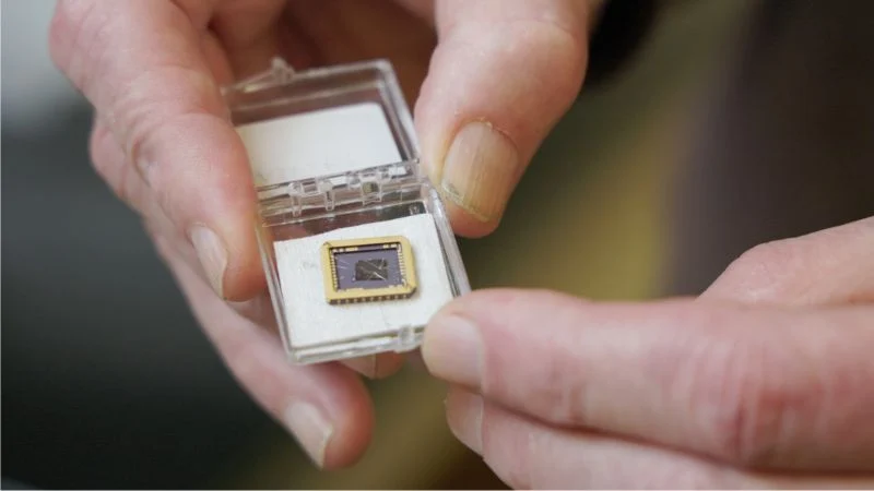
Graphene semiconductor. Image used courtesy of Georgia Tech
In groundbreaking research at Georgia Tech, scientists created the world’s first successful graphene semiconductor.
Graphene: A Semimetal
Graphene has long been known as a material with exceptional electrical properties, including high electron mobility, excellent thermal conductivity, and remarkable mechanical strength. Its single-layer structure of carbon atoms arranged in a two-dimensional honeycomb lattice enables electrons to move through it with minimal resistance, making it one of the most conductive materials known.
However, despite its huge potential, other physical limitations have prevented its use in conventional semiconductor applications.
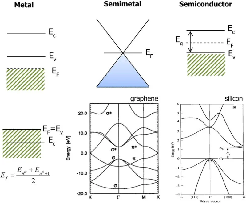
Semimetals have no bandgap. Image used courtesy of Lee et al.
In its inherent state, graphene is classified as a semimetal, meaning it does not naturally behave as a semiconductor or a metal. For a material to function effectively in electronic devices like transistors, it needs a bandgap so the material can be switched “on” and “off” through an electric field. This principle underpins the functioning of silicon-based electronics. Therefore, the principal challenge in leveraging graphene for electronic applications has been to induce this switchable characteristic, akin to silicon, without undermining its intrinsic properties.
Georgia Tech’s Graphene Research
Recently, a research team at Georgia Tech claimed to have created the world’s first graphene-based semiconductor device.
The researchers successfully showed that a well-annealed epigraphene on a specific silicon carbide crystal face can serve as a high-mobility 2D semiconductor. Specifically, the team developed semiconducting epigraphene (SEG) on single-crystal silicon carbide substrates, demonstrating a bandgap of 0.6 eV and room temperature mobilities exceeding 5000 cm2/Vs, which is significantly higher than silicon and other two-dimensional semiconductors?.
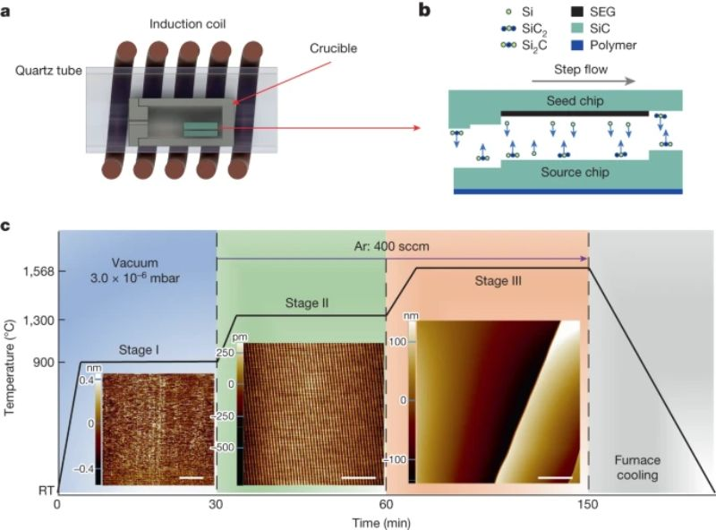
The SEG production process. Image used courtesy of Zhao et al.
The production of SEG involves a confinement-controlled sublimation (CCS) furnace where a semi-insulating SiC chip is annealed in a graphite crucible under an argon atmosphere. The temperature and rate of graphene formation are precisely controlled, with the silicon escape rate from the crucible playing a critical role.
To characterize the SEG, the team used scanning tunneling microscopy (STM), scanning electron microscopy (SEM), low-energy electron diffraction (LEED), and Raman spectroscopy. These methods allowed for a detailed examination of SEG across multiple scales, distinguishing it from bare SiC and graphene and confirming its atomic registration with the SiC substrate?.
The Potential of Semiconducting Epigraphene
The research team underscores the potential of SEG in nanoelectronics.
As a well-crystallized 2D semiconductor with a notable bandgap and high mobilities, SEG represents a major step forward for the industry in attaining the electrical benefits of materials like graphene. Future work will focus on reliably producing large terraces with suitable dielectrics, managing Schottky barriers, and developing integrated circuit schemes. Ultimately, the research team believes that SEG has the potential to become commercially viable and have a tangible impact on 2D nanoelectronics?.