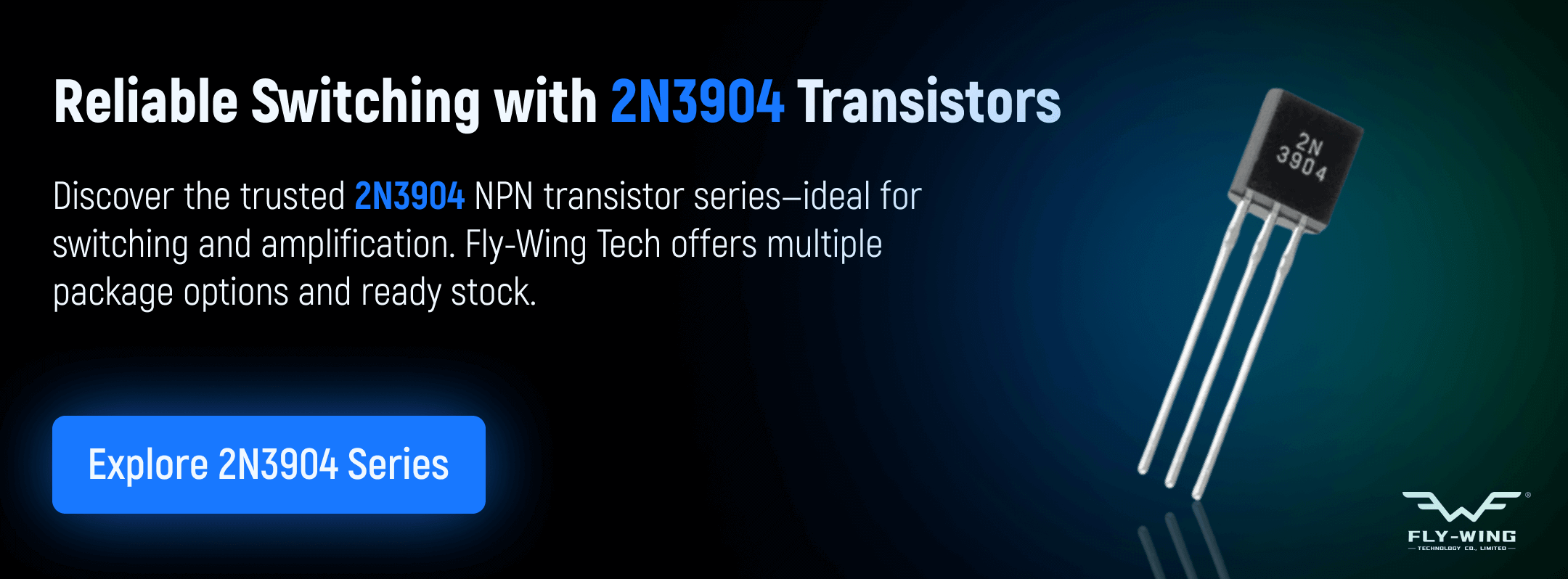
When starting out in electronics, a common problem is that sensors and microcontrollers only deliver tiny signals, while real-world components like LEDs, buzzers, or relays require more power to operate. The 2N3904 transistor solves this gap.
It is a general-purpose NPN BJT designed for switching and amplification, and for decades, it has been one of the most popular choices among hobbyists and engineers alike.
The 2N3904 transistor datasheet illustrates its versatility. With a maximum collector current of 200 mA, a collector-emitter voltage rating of 40 V, and a current gain (hFE) of approximately 100, this compact device can accept a small input and control significantly larger loads.
Its transition frequency near 300 MHz means the 2N3904 works not only for DC switching but also for higher frequency applications, including audio and RF circuits.
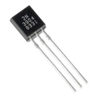
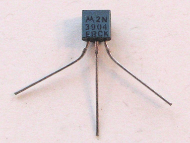
In practical use, the 2N3904 pin configuration makes it simple to integrate into breadboard projects and PCB designs. Packaged in the familiar TO-92 case, its three-pin emitter, base, and collector are clearly arranged for quick wiring.
Due to this, you will find the 2N3904 in numerous designs, from driving LEDs and operating small relays to boosting audio signals or acting as a buffer for sensors.
In this guide we will cover the 2N3904 transistor pinout, its key specifications from the 2N3904 datasheet, how it works in practice, and beginner friendly circuits you can build right away.
What is 2N3904 Transistor?
The 2N3904 Transistoris a widely used NPN bipolar junction transistor designed for general-purpose applications. It belongs to the family of small-signal transistors that are used to control or amplify electrical signals in everyday circuits.
In practice, the 2N3904 works as a tiny electronic switch or amplifier. When a small input is applied at the base, it allows a larger current to pass from the collector to the emitter.
This simple principle makes it useful in a variety of projects, from turning LEDs on and off to boosting weak signals from sensors or microphones.
Physically, the transistor is most often found in the compact TO-92 plastic package, with three clearly defined pins: emitter, base, and collector.
Its popularity comes from being inexpensive, easy to use, and compatible with breadboard setups as well as permanent PCB designs.
Because of these qualities, the 2N3904 has become a go-to choice for students, hobbyists, and engineers alike, often serving as one of the first transistors beginners learn to work with.
2N3904 Transistor Pinout Diagram
When looking at the flat face of the transistor (with the leads pointed downward), the pins from left to right are Emitter, Base, and Collector.
Most TO-92 transistors, including the 2N3904, have a flat side or notch to show orientation. Its three pins are Emitter, Base, and Collector.
The Base controls the transistor, the Collector is where current enters, and the Emitter is where current leaves (usually to ground in NPN use).
In the standard TO-92 package, with the flat side facing you, the pins from left to right are Emitter, Base, Collector. Always confirm the order in the datasheet before wiring.

| Pin Number | Pin Name | Function |
| 1 | Emitter (E) | Connected to ground or negative side of circuit. Emits electrons (current flows out of this terminal). In an NPN, the emitter is typically at the lowest potential. |
| 2 | Base (B) | Controls the transistor’s biasing. A small current or voltage at the base activates the transistor. Think of it as the “gate” for current flow between collector and emitter. |
| 3 | Collector (C) | Connected to the load and the positive supply. Collects electrons from the emitter when the transistor is on. This is the terminal through which the main controlled current flows into the transistor. |
In practical use, knowing the pinout is crucial for wiring the transistor correctly.
If you hold the transistor such that the flat face is towards you and pins facing downward, the leftmost lead is the Emitter, the middle is the Base, and the rightmost is the Collector.
2N3904 Features and Specifications
The 2N3904 is a silicon NPN bipolar junction transistor (BJT) designed for low-power switching and signal amplification. Its datasheet defines both the absolute maximum ratings (limits you should never exceed) and the electrical characteristics (the typical values you can expect in use).
Transistor Type and Package
- Type: NPN bipolar junction transistor made from silicon. It works when the base–emitter junction is forward biased, allowing current amplification.
- Package: Supplied mainly in the TO-92 plastic through-hole package. Also available in surface-mount versions such as MMBT3904 (SOT-23) and PZT3904 (SOT-223).
Maximum Voltages (Absolute Ratings)
- VCEO (Collector to Emitter voltage): 40 V
This is the maximum voltage allowed across collector and emitter when the base is open. Going beyond this risks breakdown. - VCBO (Collector to Base voltage): 60 V
The maximum voltage the collector–base junction can handle with the emitter open. - VEBO (Emitter to Base voltage): 6 V
The maximum reverse voltage allowed between emitter and base. Exceeding this can damage the base–emitter junction.
Maximum Current
- IC (Collector current): 200 mA continuous
This is the highest steady current the transistor can pass through collector to emitter. In practice, staying below 150 mA is recommended for reliability. - IB (Base current): about 5 mA recommended maximum
This keeps the base–emitter junction safe while still allowing the transistor to saturate when switching loads.
Power Dissipation
- PD (Total device dissipation): 625 mW at 25 °C in free air
- PD (case-mounted): 1.5 W at 25 °C
These values describe how much heat the transistor can safely dissipate. If it gets too hot, performance drops and reliability suffers. Always allow for cooling or derating if operating at higher temperatures.
DC Current Gain
- hFE (DC current gain): typically 100, maximum around 300
This is the ratio of collector current to base current. For example, if IB = 1 mA and hFE = 100, then IC ≈ 100 mA. Gain depends on operating conditions and tends to drop at very low or very high currents.
Formula:
\[ h_{FE} = \frac{I_C}{I_B} \]
Saturation Voltages
- VCE(sat): 0.2 to 0.3 V
When the transistor is fully on, the collector–emitter voltage drop is small, making it efficient as a switch. - VBE(sat): 0.65 to 0.95 V
The base–emitter voltage in saturation. This is why about 0.7 V is needed at the base to turn it on.
Transition Frequency
- fT (Transition frequency): around 300 MHz
This is the frequency where the current gain drops to 1. In practical terms, it means the 2N3904 can handle not just DC and audio signals but also RF circuits up into the VHF band.
Other Important Specs
- Base–Emitter on voltage: about 0.65–0.7 V under normal conduction.
- Leakage currents: typically below 50 nA, meaning the transistor wastes almost no current when switched off
- Input capacitance (Cibo): ≤ 8 pF
- Output capacitance (Cobo): ≤ 4 pF
These small capacitances help the transistor switch quickly.
Learn more about their characteristics in the official 2N3904 datasheet.
Working Principle of 2N3904 Transistor
The 2N3904 is a bipolar junction transistor (BJT), which means it operates based on current flow through two PN junctions inside the device.
It consists of three structural regions:
- Emitter (N-type) – heavily doped to supply carriers (electrons).
- Base (P-type) – very thin and lightly doped so carriers can cross easily.
- Collector (N-type) – moderately doped and larger, designed to collect carriers.
In an NPN transistor like the 2N3904, the emitter–base junction acts like a diode (forward biased when active), while the base–collector junction is reverse biased under normal operation.
Base–Emitter Junction (Forward Bias)
When the base is made about 0.6–0.7 V more positive than the emitter, the base–emitter junction conducts.
A small base current (IB) begins to flow. Below this voltage, the transistor remains “off” and IB is almost zero.
Collector–Emitter Current Control
Once IB flows, electrons from the emitter are injected into the thin base region. Most of these are swept into the collector because the base is lightly doped and very thin.
This creates a larger collector current (IC). The relationship is defined by the transistor’s current gain:
If hFE ≈ 100, then a base current of 1 mA can control a collector current of about 100 mA.
Active Region (Amplification)
In the active region, the transistor behaves as an amplifier. Here:
\[ I_C \approx \beta \times I_B \]
where β (beta) is another name for hFE. The collector maintains a moderate voltage above the emitter, and the transistor is only partially on.
This is the region used in analog amplification (for example, boosting an audio signal). Proper biasing resistors are needed to keep the transistor in this mode and avoid distortion.
In the active region, the collector current follows the base current according to the current gain (hFE). Learn more about BJTs in detailed references.
Saturation and Cut-Off (Switching)
For digital switching, the 2N3904 operates in two extreme states:
- Cut-Off: Base not forward biased (VB < 0.6 V). IB ≈ 0, so IC ≈ 0. The transistor is OFF — like an open switch.
- Saturation: Base is strongly driven with current. Increasing IB further does not increase IC significantly. The transistor is fully ON, IC is limited by the load and supply, and VCE drops very low (~0.1–0.3 V). It acts like a closed switch.
Rule of thumb for saturation:
\[I_B \approx \frac{I_C}{10} \ \text{to} \ \frac{I_C}{20} \]
Using the Transistor in Circuits
As a Switch
- Input HIGH → base current flows → transistor saturates → load current flows from collector to emitter.
- Input LOW → no base current → transistor cuts off → load current stops.
As an Amplifier
- Base biased partially on → transistor in active region.
- Small variations at the base cause larger variations in collector current, producing voltage gain across a collector load resistor.
Base Resistor Calculation
To prevent damaging the base–emitter junction, a resistor is always used in series with the base. The calculation is:
\[ R_B = \frac{V_{in} – V_{BE}}{I_B} \]
Example: If Vin = 5 V, VBE ≈ 0.7 V, and desired IB = 1 mA:
\[ R_B = \frac{5 – 0.7}{0.001} \approx 4300 \ \Omega \]
So, a standard 4.7 kΩ resistor would be suitable.
2N3904 Transistor Applications and Use Cases
Given its characteristics, the 2N3904 transistor is one of the most versatile building blocks in electronics.
From switching logic signals to amplifying audio and even handling radio frequencies, it fits into countless designs.
Below are the most common 2N3904 applications.
Switching and Digital Control
One of the simplest uses of the 2N3904 is as a switch. A microcontroller output, such as from an Arduino, cannot directly power motors, buzzers, or relays because of current limits.
By feeding a small base current (through a resistor) into the 2N3904, the transistor saturates and allows the collector-emitter path to conduct.
This lets it control larger loads such as LEDs, small relays, or lamps. In effect, the transistor acts as an interface between logic-level signals and higher-current devices.
LED and Relay Drivers
The 2N3904 transistor datasheet shows a maximum collector current of 200 mA, which is sufficient for small relays and multiple LEDs.
That makes it a go-to driver for indicator lights, LED arrays, and low-power relays. In relay circuits, a protective diode is always placed across the coil to absorb back-EMF when switching off.
Amplifiers (Audio and Signal)
Configured in amplifier circuits, the 2N3904 can boost weak analog signals. Common amplifier topologies include:
- Common emitter amplifiers, which provide voltage gain with phase inversion.
- Emitter followers (common collector), which buffer signals by offering current gain without voltage gain.
- Darlington pairs, where two transistors combine to deliver very high gain.
With a typical gain (h_FE) around 100 and a transition frequency of about 300 MHz, the 2N3904 is well suited for audio amplifiers, microphone preamps, and sensor signal conditioning.
For example, it can raise a 50 mV audio signal to a few volts, strong enough to feed a speaker driver or another stage of a circuit.
Oscillators and Timers
The 2N3904 also plays a role in waveform generation and timing circuits.
Paired with resistors and capacitors, it can form an astable multivibrator that blinks LEDs alternately, or act as part of a flip-flop or pulse generator.
Its fast switching speed makes it suitable for producing square waves at audio or ultrasonic frequencies. Hobby projects like LED flashers, clock circuits, or tone generators often rely on the 2N3904 for this purpose.
Radio Frequency (RF) Circuits
With a transition frequency near 300 MHz, the 2N3904 is capable of handling RF signals in the HF and VHF bands.
While it is not a high-power RF device, it works well in low-power RF amplifiers, oscillators, and small transmitter circuits.
It is often paired with its complementary PNP counterpart, the 2N3906, in push-pull oscillator designs.
Sensor Interfaces and Miscellaneous Uses
The 2N3904 is a natural fit for sensor circuits, acting as a switch or amplifier for inputs like light, sound, or temperature.
For instance, an LDR (light-dependent resistor) can feed into the transistor’s base to make a simple light-controlled switch.
Similarly, sound-activated circuits or temperature sensors often use the 2N3904 to provide gain or switching action.
Its high input impedance at the base and good current gain make it a flexible choice for sensor interfacing.
2N3904 Transistor Example Circuits
To solidify our understanding, let’s go through a couple of example circuits featuring the 2N3904 transistor.
These examples demonstrate the two primary modes of operation: as a switch and as an amplifier.
They are simplified for beginners, so you can try building them on a breadboard.
1. Simple LED Flasher Circuit using 2N3904
This example shows how you can use the 2N3904 transistor to build a very simple LED flasher circuit.
It’s a beginner-friendly project that demonstrates how a transistor can drive and control loads like LEDs.
| S. No | Component | Value / Type | Quantity |
| 1 | Breadboard | – | 1 |
| 2 | LED | 5 mm (1 normal LED + 1 self-flashing LED) | 2 |
| 3 | Battery | 6 V | 1 |
| 4 | Transistor | 2N3904 NPN | 1 |
| 5 | Resistor | 10 kΩ, 4.7 kΩ, 1 kΩ | 1 each |
| 6 | Capacitor | 100 µF | 1 |
- Pin 1 (Emitter): Connected to ground.
- Pin 2 (Base): Bias control pin.
- Pin 3 (Collector): Connected to the load (in this case, the LED).
For more details, see the 2N3904 transistor datasheet (dimensions, pin orientation, and electrical ratings).
LED Flasher Circuit Diagram
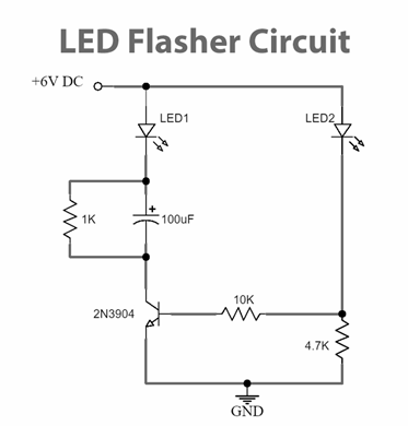
Working Explanation
The circuit uses a self-flashing LED as the timing element. This LED contains a built-in oscillator circuit that blinks on and off at a set frequency.
Each time the self-flashing LED turns on, it sends a small current into the base of the 2N3904 transistor.
The transistor then switches ON, allowing a larger current to flow from the collector to the emitter, which drives the second LED (a normal super-bright LED).
As the self-flashing LED turns off, the base drive disappears, the transistor cuts off, and the second LED goes dark. This creates a synchronized flash effect.
The resistor (1 kΩ) sets the current through the self-flashing LED and, in turn, influences the flash rate of the second LED. Adjusting this resistor changes how fast the LED blinks.
Key Notes:
- The 2N3904 transistor acts as a driver, ensuring the super-bright LED gets enough current without overloading the self-flashing LED.
- You can power the circuit with a simple 6 V battery pack or DC supply.
- Any small NPN transistor (like 2N2222 or BC547) can be substituted if needed.
2. Simple Amplifier Circuit using 2N3904
Amplifiers are among the most common applications of transistors. They take a weak input signal and boost it into a stronger output.
In this tutorial, we’ll build a simple audio amplifier circuit using the 2N3904 transistor along with a supporting transistor pair for improved gain. This project is beginner-friendly and demonstrates how a basic transistor amplifier works in a common-emitter configuration.
| S. No | Component | Value / Type | Quantity |
| 1 | NPN Transistor | 2N3904 | 2 |
| 2 | NPN Transistor | 2SC1815 | 1 |
| 3 | Resistors | 3.3 MΩ, 820 kΩ, 39 kΩ, 10 kΩ, 330 Ω | 1 each |
| 4 | Electrolytic Capacitors | 1 µF, 47 µF, 220 µF | 1 each |
| 5 | Speaker | 0.5 W | 1 |
| 6 | Battery | 6 V DC | 1 |
Amplifier Circui Diagram

Working Explanation
The circuit uses three transistors arranged to provide step-by-step amplification:
Input stage (Q1 – 2N3904)
- The input signal (audio or weak AC) passes through capacitor C1.
- The capacitor removes any DC component, allowing only the AC signal to enter the base of Q1.
- Q1 is configured as a common-emitter amplifier, where the base receives the input, the collector provides the output, and the emitter is grounded.
- A voltage divider bias formed by R1 and R2 sets the proper base voltage for Q1, keeping it in the active region.
Intermediate gain stage (Q2 and Q3 – 2N3904 + 2SC1815)
- The amplified signal from Q1’s collector is still relatively weak.
- It is fed into Q2 and Q3, which are connected as a Darlington pair.
- In a Darlington configuration, two transistors act together, giving a very high effective current gain (hFE ≈ hFE1 × hFE2).
- This ensures the signal is strong enough to drive the load (the speaker).
Output stage (Speaker + C3)
- The final amplified signal passes through capacitor C3 (220 µF) before reaching the speaker.
- This capacitor blocks any DC offset, letting only the amplified AC audio signal reach the speaker.
- The result is a louder, clearer version of the original weak input.
Key Notes:
- The 2N3904 handles the first amplification stage, providing a moderate voltage gain.
- The Darlington pair (Q2 and Q3) provides the current amplification, driving the speaker efficiently.
- Capacitors are essential here: C1 filters the input, C2 (47 µF) may stabilize biasing, and C3 couples the final amplified signal to the speaker.
For techniques on designing reliable transistor amplifiers, check out our guide: How to Design Stable Discrete Transistor Circuits
2N3904 Transistor vs Other Transistors
The 2N3904 is one of the most widely used small-signal NPN transistors, but it’s not the only one in this category.
Several other transistors share similar specifications and can often serve as substitutes.
Knowing the differences helps you choose the right one for your project or find reliable replacements.
2N3904 vs 2N2222
The 2N2222 is just as famous among hobbyists as the 2N3904. The main difference lies in current handling:
- 2N3904: Collector current up to 200 mA
- 2N2222: Collector current up to 600–800 mA (depending on version)
Both are rated around 40 V VCEO (though some 2N2222 datasheets list 30 V). Their gain and switching speeds are similar, though the 2N3904 often has a slightly higher transition frequency (~300 MHz vs ~250 MHz).
The 2N2222 is often found in a metal TO-18 can package, while the PN2222A is the TO-92 plastic version. Pinout is the same as the 2N3904 (E-B-C).
The 2N2222 is another hobbyist favorite, often packaged in TO-18 metal cans. Learn more about 2N2222 here.
When to use:
- Use the 2N3904 for currents under 200 mA.
- Choose the 2N2222 for heavier loads (relays, motors, multiple LEDs).
2N3904 vs 2N4401
The 2N4401 is like a higher-current version of the 2N3904.
- Both rated around 40 V VCEO
- 2N3904: 200 mA collector current
- 2N4401: 600 mA collector current
Gain (hFE) is in a similar range, with the 2N4401 sometimes showing slightly higher gain at medium currents. Pinout is the same (E-B-C in TO-92).
When to use:
- 2N3904: Low-power tasks.
- 2N4401: A drop-in substitute when you need more current capacity.
2N3904 vs BC547 / BC548
The BC547 and BC548 are very common in European circuits and are quite close in function to the 2N3904.
- VCEO: ~45–50 V (slightly higher than 2N3904)
- IC max: ~100 mA (lower than 2N3904)
- hFE: Can range from 110 to 800 depending on subtype (B, C versions have higher gain)
The pinout is reversed compared to American types. In BC547/548 (looking at the flat side), pins are C-B-E left to right, while the 2N3904 is E-B-C.
BC547/548 are fine substitutes in low-current circuits, but always double-check pin orientation.
2N3904 vs 2N3906 (PNP Complement)
The 2N3906 is the PNP complement of the 2N3904.
- Very similar specs (40 V, 200 mA).
- Opposite polarity of operation.
Use the 2N3906 for PNP configurations, such as high-side switching or push-pull amplifier stages. Together, the 2N3904 and 2N3906 form a complementary pair often used in audio and signal circuits.
Final Thoughts
The 2N3904 transistor continues to be a staple for hobbyists, students, and engineers. Its simple pinout, solid specifications, and wide availability make it perfect for learning switching concepts, designing amplifiers, or experimenting with LED drivers and small-signal circuits. Understanding its datasheet parameters and working principles ensures you can apply it confidently across a variety of projects.
And when your circuits demand more current or complementary operation, there are plenty of related transistors like the 2N2222, 2N4401, or the PNP 2N3906.
Ready to start building? You can order the 2N3904 in different package types and variants directly from Flywing-Tech:
👉 Visit Flywing-Tech.com to explore our complete catalog of transistors, connectors, solar components, and electronic accessories to power your next project.
Frequently Asked Questions [FAQ]
What is the maximum voltage and current of the 2N3904?
It can handle 40 V (VCEO) and 200 mA (IC) at maximum. For safe operation, keep it below ~30 V and ~100–150 mA continuous. If you need more power, use a 2N2222, 2N4401, or a MOSFET.
Can I use a 2N3904 to drive a motor or relay?
Yes, but only small motors or relays (tens of mA up to ~100 mA). Always use a flyback diode across coils. For larger loads (0.5–1 A), use a stronger transistor or MOSFET.
Why is a base resistor needed?
The base–emitter junction acts like a diode (~0.7 V). Without a resistor, the base would draw excessive current and damage the transistor or driver. Use:
\[RB = (Vin – 0.7 V) / IB\]
Rule of thumb: set \[IB ≈ IC / 10\] for switching.
Can the 2N3904 be used in RF circuits?
Yes. With a transition frequency (fT) of ~300 MHz, it works well for HF/VHF amplifiers, oscillators, and low-power transmitters. It is not suitable for GHz-range signals like WiFi.
What is the difference between 2N3904 and 2N2222?
Both are NPN BJTs rated ~40 V. The 2N3904 handles up to 200 mA, while the 2N2222 can handle 600–800 mA. Pinout is the same (E-B-C). Use 2N3904 for small loads, 2N2222 for higher current.
What is the PNP equivalent of 2N3904?
The 2N3906. It has nearly identical ratings (40 V, 200 mA) but opposite polarity. Use it for PNP circuits such as high-side switches or complementary amplifier stages.
How can I test if my 2N3904 is working?
With a multimeter in diode mode:
- Base → Emitter ≈ 0.6–0.7 V forward drop.
- Base → Collector ≈ 0.6–0.7 V forward drop.
- Reverse directions should read open. Collector ↔ Emitter should be open with no base current.
If results differ (shorts or opens), the transistor is bad. A component tester can also measure hFE and identify pinout automatically. For step-by-step transistor and electronics testing tutorials, see our Component Testing Guide.