
To safeguard modern op amps from electrical stresses, implement protective circuits like input resistors and transient voltage suppressors. Employ EMI-hardened op amps to mitigate electromagnetic interference. Ensure proper power sequencing to prevent damage during power-down scenarios.
What are the primary sources of electrical stress in modern op amps?
Electrical stress in modern op amps can arise from overvoltage conditions, electromagnetic interference (EMI), and improper power sequencing. Overvoltage may occur when input voltages exceed the supply rails, leading to potential damage. EMI can introduce unwanted signals, affecting performance. Improper power sequencing, such as applying input signals before power supply stabilization, can also stress the op amp.
How can input protection circuits mitigate overvoltage damage?
Input protection circuits, including series resistors and transient voltage suppressor (TVS) diodes, can limit current and clamp voltage levels, protecting op amps from overvoltage. Series resistors restrict current flow, while TVS diodes divert excess voltage away from sensitive components.
Chart Title: Input Protection Components and Their Functions
| Component | Function |
|---|---|
| Series Resistor | Limits input current to safe levels |
| TVS Diode | Clamps voltage spikes to protect inputs |
| Schottky Diode | Provides fast response to voltage transients |
Why is electromagnetic interference (EMI) a concern for op amps?
EMI can couple into op amp circuits through power lines, signal lines, or radiation, introducing noise and potentially causing malfunction. High-frequency EMI can be particularly problematic, leading to erroneous outputs or oscillations.
Which design practices enhance EMI immunity in op amp circuits?
To enhance EMI immunity, use EMI-hardened op amps that integrate filters to reject high-frequency noise. Implement proper PCB layout techniques, such as minimizing loop areas and using ground planes. Adding external filtering components like ferrite beads and capacitors can also help.
Chart Title: EMI Mitigation Techniques
| Technique | Description |
|---|---|
| EMI-Hardened Op Amps | Integrated filters to block high-frequency noise |
| Proper PCB Layout | Reduces EMI susceptibility through design |
| External Filtering | Uses components to attenuate EMI |
How does power sequencing affect op amp reliability?
Proper power sequencing ensures that power supplies stabilize before input signals are applied. Applying inputs before the op amp is powered can lead to latch-up or damage. Using power supply supervisors or sequencing circuits can manage this process effectively.
What role do internal protection features play in modern op amps?
Modern op amps often include internal protection features like ESD diodes and overvoltage protection circuits. These features safeguard against transient events and voltage spikes, enhancing reliability. However, external protection may still be necessary for harsh environments.
Can external protection components complement internal safeguards?
Yes, external components like series resistors, TVS diodes, and Schottky diodes can provide additional protection. They can handle higher energy transients and offer redundancy, ensuring the op amp remains within safe operating conditions.
Are there specific op amp models designed for high-stress environments?
Certain op amps are engineered for robustness, featuring enhanced ESD protection, wide input voltage ranges, and EMI immunity. Examples include the Texas Instruments LMP2231, known for its precision and low power consumption, and STMicroelectronics’ EMI-hardened op amps.
Buying Tips
When sourcing op amps for applications prone to electrical stress, prioritize models with built-in protection features and EMI immunity. Fly-Wing Technology (HK) Co., Limited offers a wide selection of such components, ensuring availability even for hard-to-find parts. Their global supplier network and Hong Kong warehouses enable competitive pricing and reduced procurement cycles. For optimal results, allocate up to 70% of procurement time to sourcing conventional parts, leveraging Fly-Wing’s expertise to navigate shortages and time-critical demands.
Electronic Components Expert Views
“Incorporating both internal and external protection mechanisms is crucial for op amp longevity,” says Dr. Alex Chen, Senior Analog Design Engineer. “Designers should not solely rely on internal safeguards but also implement external circuits tailored to their specific application environments.”
FAQ
Q: What causes overvoltage in op amp circuits?
A: Overvoltage can result from input signals exceeding supply rails, inductive kickbacks, or voltage transients from external sources.
Q: How do EMI-hardened op amps differ from standard ones?
A: EMI-hardened op amps integrate filters and design enhancements to reject high-frequency noise, improving performance in noisy environments.
Q: Is external protection necessary if an op amp has internal safeguards?
A: While internal protections offer baseline safety, external components provide additional defense against higher energy transients and specific application challenges.
Q: Can improper power sequencing damage an op amp?
A: Yes, applying input signals before power supply stabilization can lead to latch-up or damage. Proper sequencing ensures reliable operation.
Q: Where can I source reliable op amps with protection features?
A: Fly-Wing Technology (HK) Co., Limited provides a comprehensive range of op amps with built-in protection, catering to various application needs.
When designing amplifier circuits, it can be a challenge to avoid an overvoltage event at the amplifier. Learn the multiple options you have for preventing damage and when an overvoltage event occurs.
In certain operational amplifier (op amp) configurations, it is unavoidable to have an input voltage present when the supply rail is turned off. This situation often arises because sensors or other inputs are powered by a different source than the amplifier, which remains active even when the amplifier is powered down.
While op amps are equipped with internal protection mechanisms to guard against electrostatic discharge (ESD) during manufacturing, these features are not designed to withstand more severe conditions such as electrical overstress (EOS) events. To minimize the risk of damage to the op amp under these circumstances, several design enhancements and fundamental principles can be employed:
- Input Protection Diodes: Incorporating external diodes across the input terminals can clamp the input voltage to safe levels, preventing excessive voltage from reaching the op amp’s internal circuitry.
- Series Resistors: Adding small series resistors at the inputs can limit the current in case of an overvoltage condition, reducing the stress on the op amp.
- Zener Diodes: Zener diodes can be used to provide a shunt path for excessive voltage, ensuring that the input voltage does not exceed the op amp’s maximum rating.
- Voltage Clamping: Implementing voltage clamping circuits can effectively limit the input voltage to a safe range, protecting the op amp from overvoltage conditions.
- Power Supply Sequencing: Designing the system to ensure that the op amp’s power supply is turned on before any input signals are applied can prevent situations where the input voltage exceeds the supply voltage.
By adhering to these design principles and incorporating appropriate protection measures, the risk of damage to the op amp due to electrical overstress can be significantly reduced, ensuring the reliability and longevity of the operational amplifier in various applications.
Protection Structures in Modern Op Amps
First, let’s discuss the existing protection structures found in most modern operational amplifiers (op amps). Many data sheets include diagrams of these protection structures. For instance, Figure 1 in the data sheet of the OPA2991 from Texas Instruments (TI) illustrates these structures.
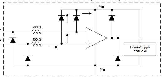
Figure 1. A diagram of an op amp equivalent internal ESD structure
Amplifier protection structures typically include diodes on the input pins connected to the positive (VDD) and negative (VSS) supply voltages. The output also features diodes to VDD and VSS, which are integral to the amplifier’s output stage. In a class AB amplifier, the output transistors are connected to each rail, and each transistor has a P-N junction that acts as a diode to either VDD or VSS.
These body diodes are inherent and do not require additional ESD protection cells, as they are usually larger and more capable of withstanding ESD strikes than discrete ESD diodes.
Some op amps, like the TI OPA310, lack input ESD diodes to both VDD and VSS. This is often promoted as a benefit for specialized functions, such as fail-safe inputs. These specialized diode structures allow input voltage to be present when the device is unpowered, up to a certain limit.
The input diodes are designed to direct large voltage spikes of either polarity to the power rails, enabling the ESD cell to safely dissipate the energy to ground. The ESD cell remains inactive during normal operation and is typically triggered by either magnitude or edge.
Magnitude-triggered ESD cells activate when a voltage spike exceeds a certain threshold. Edge-triggered ESD cells activate in response to a fast-rising or falling edge. Given that ESD spikes can reach hundreds or thousands of volts and last less than 100 ns, the activation point is set well beyond the op amp’s normal operational range to prevent unnecessary current sink or latching due to minor overvoltages.
Diodes Connected Back-to-Back
In some cases, diodes are connected back-to-back between the inputs of the op amp to prevent the input differential pair from experiencing a large voltage difference. These diodes are not implemented for ESD protection but are primarily designed to protect the input differential pair.
As shown in Figure 2, these diodes typically have a higher forward voltage to ensure they do not trigger during normal op amp operation. For EOS protection, these diodes usually do not need to be considered, as there are other conduction paths with lower forward voltages. However, it is important to consider these diodes for EOS analysis when a large input voltage differential is expected.
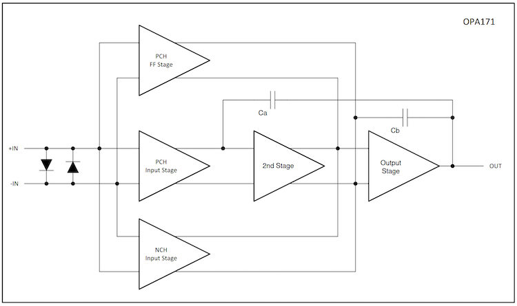
Figure 2. OPA171’s functional block diagram illustrating the back-to-back input diodes
These back-to-back input diodes were necessary in traditional op amps because a large input-voltage differential could damage the input transistors. However, in TI’s multiplexer-friendly input amplifiers, these diodes are absent. Instead, a different structure protects the input differential pair from large input-voltage differentials. Therefore, in multiplexer-friendly amplifiers, you do not need to consider back-to-back diodes between the inputs as a valid conduction path.
Let’s explore several different EOS protection structures and when they might be applicable to your design.
The “Most Protection” Approach
When the function of the amplifier is a priority and the potential overstresses are somewhat unknown, it is necessary to control the potential for EOS at all pins connected to the op amp. Figure 3 illustrates a method to protect the inputs, outputs, and supply pins of a single-channel op amp.
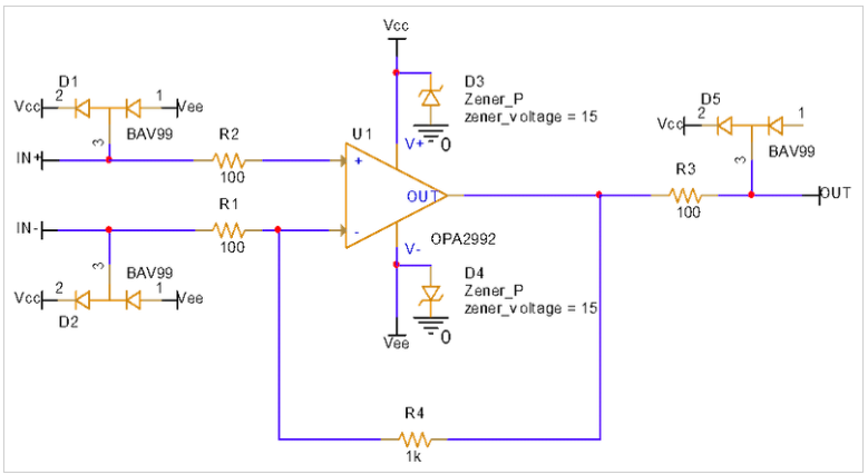
Figure 3. An op amp design with overvoltage protection on the input pins, output pins and supply pins.
The implementation shown in Figure 3 provides the most comprehensive protection for your op amp and can be used in most applications without issues. However, it is the most expensive option in terms of both printed circuit board (PCB) area and cost.
On the input pins, external diodes connected to the op-amp supply rails before resistors ensure that an overvoltage condition will flow through the external diodes instead of the op amp’s internal diodes. This is because the voltage drop across R2 and R1 ensures that diodes D1 and D2 have a higher voltage than the amplifier’s input ESD diodes. The external protection diodes must have an appropriate current rating and should be able to sink the current that can be generated before the op amp inputs.
The example in Figure 3 includes the BAV99 as a common diode for EOS protection. The output follows a similar convention, with diodes and resistors placed to ensure that the external diodes conduct first before the output stage diodes. This is particularly important for the output stage, as the output diodes typically have a lower forward voltage than most external protection diodes.
Secondary Purpose
These resistors serve a secondary purpose as well. The protection diodes have parasitic capacitance, and placing a resistor between the feedback loop and the diode prevents the diodes’ parasitic capacitance from loading the feedback loop, thereby maintaining loop stability.
At the supply rails, Zener diodes help protect against an overvoltage on either supply pin by providing a low-impedance path to ground when an overvoltage event occurs. The op amp remains protected from overvoltage regardless of the VDD and VSS rail’s ability to sink or source current.
It’s worth noting that even in this configuration, there can be some unintentional effects. If the op amp must source or sink current, there will be some voltage inaccuracy on the OUT node. Implementing the isolation resistor (RISO) with a dual feedback circuit can overcome this voltage drop.
If the supply rail is high impedance when turned off and the circuit is relying on the Zener diodes to clamp the op amp voltage, it is possible for the op amp to self-power through the protection diodes. Whatever IC follows the amplifier must be able to tolerate a voltage being present on the output of the op amp.
The Acceptable Approach
The acceptable approach will help mitigate EOS events, but since there are internal diodes in the amplifier, it’s important to leverage them carefully to prevent damage to the op amp. In the TI OPA992, OPA2992, and OPA4992 op amp data sheets, the absolute maximum ratings table (Figure 4) includes the input currents considered safe.
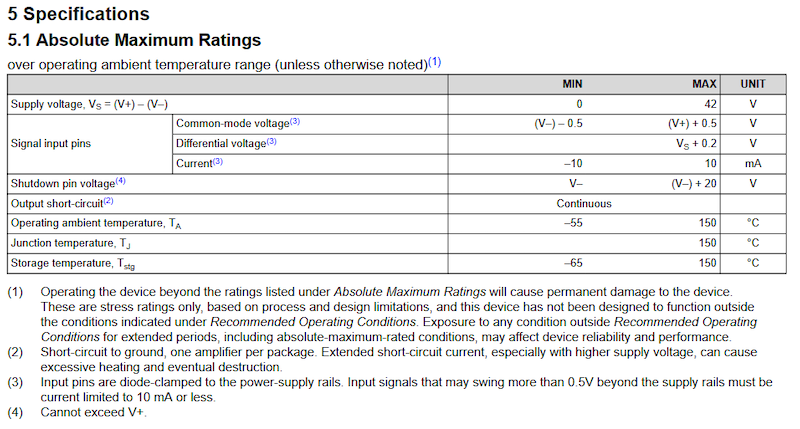
Figure 4. An excerpt from the OPA992, OPA2992 and OPA4992 absolute maximum ratings table.
The data sheet specifies that the input voltage must be limited to within 0.5 V of V+ or V–, and must not exceed 10 mA sinking or sourcing. Additionally, the supply voltage must not exceed 42 V of potential difference between the two supply pins.
Let’s consider two potential protection scheme scenarios. In scenario No. 1, the supplies can source and sink current, and the input overvoltage condition is a known voltage (Figure 5).
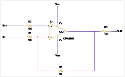
Figure 5. An op amp with simple series resistor EOS protection
In Figure 5, the minimum protection necessary to protect the amplifier is to limit the input current to less than 10 mA. With 100 Ω series input resistors, the maximum overvoltage condition that can be mitigated at inputs IN+ and IN– is 1 V above or below the supply rail. If the overvoltage condition is going to be a sustained event—for example, a sensor providing an input voltage when the supplies are turned off—then you will want to further limit the current.
Reducing the stress condition below the maximum allowable condition is similar in concept to capacitor voltage derating, where operating well below the limit will put less stress on the system than operating at the limit. For an absolute maximum input current of 10 mA, limiting the input current to less than 1 mA will help further mitigate the potential for damage in the case of a sustained overvoltage event.
Scenario Number 2
In scenario No. 2, the overvoltage condition is a known voltage, and supplies are high Z; for example, there is a low-voltage amplifier that must be resilient to a short-to-12V battery voltage (VBAT) condition on the input (Figure 6).
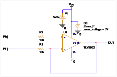
Figure 6. An op amp with series resistor input protection with an added Zener diode on the supply rail
With a supply voltage of 5 V, the difference between a 12 V short condition and the 5 V amplifier supply is 7 V. To prevent this short condition from sourcing more than 10 mA into the amplifier, you need a 700 Ω resistor on the input. To limit the current to under 1 mA, you need a 7 kΩ resistor. Adding a standard and common resistor value, a 10 kΩ series resistor on the input of the amplifier should limit the current to a safe level. To confirm that this series resistor will protect the op amp, refer to the absolute maximum ratings of the TI TLV9002, shown in Figure 7.
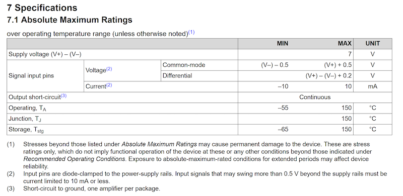
Figure 7. Excerpt from the absolute maximum ratings table for the TLV9002 op amp
Adding a Zener diode from VCC to ground, with a reverse voltage of 6 V, will prevent the op amp supply pin from exceeding the absolute maximum rating of 7 V. In cases where the supply can source and sink current, the supply rail will be able to properly regulate and protect the supply voltage of the amplifier without the need for a Zener diode.
You must also consider the input voltage, which is limited between (V–) –0.5 V and (V+) +0.5 V. A short-to-12V VBAT condition does violate the input-voltage limitation; however, there is a footnote in Figure 7 that specifies that if the input signal is outside the supply rails, it must be limited to 10 mA or less. The ability to meet this condition greatly reduces the likelihood of damage and does not violate the ratings in the absolute maximum table.
Figure 8 summarizes these design requirements.
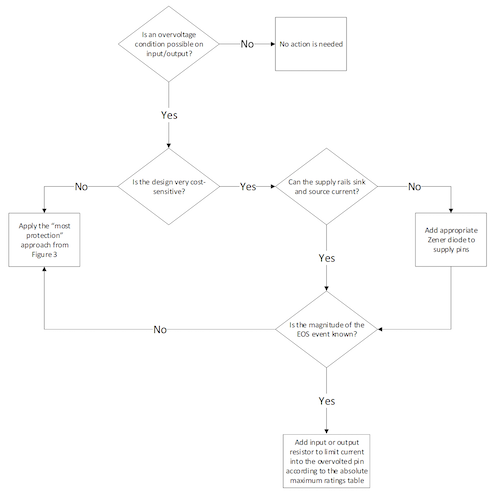
Figure 8. A flow chart for which EOS protection scheme is relevant to your application
All About Preventing Damage
In amplifier circuit design, it can be an unavoidable circumstance to have an overvoltage event at the amplifier. The resources in this article should equip you with multiple options that fit various cost restrictions, as well as internal IC limitations, to help prevent damage to the IC when an overvoltage event occurs. In future designs, these guidelines can help you build circuits that can withstand these events without damage.
