What is the CD4017 IC?
CD4017 is a decade counter and decoder IC which has a 5-bit Johnson counter with decoding logic that can provide 10 sequential decoded outputs from the input clock signal. At a time, only one output is activated. On each rising clock edge, the active output shifts towards the next pin. After the 10th output, the IC resets itself and starts from the beginning again. No programming is required for its operation.
| Parameter | Value / Range |
|---|---|
| Supply Voltage (VDD) | 3 V to 15 V (some variants to 18 V) |
| Logic Family | CMOS (4000B series) |
| Counter Type | 5-stage Johnson counter with decoder |
| Number of Outputs | 10 decoded outputs (Q0–Q9) |
| Max Clock Frequency | Up to 10 MHz (voltage dependent) |
| Propagation Delay | ~100 ns at 15 V (slower at lower VDD) |
| Static Current Draw | Microwatt range (typ. < 1 µA static) |
| Clock Input Type | Schmitt-triggered (built-in pulse shaping) |
| Reset Pin Logic | Active-HIGH |
| Clock Enable Logic | Active-HIGH inhibit (LOW = counting enabled) |
| Carry Out Function | Goes HIGH for 5 of every 10 clock cycles |
| Package Options | 16-pin PDIP, SOIC-16 |
| Output Drive | Each output can directly drive an LED with resistor |
The Sequential Switching Problem
You want to have LED lights sequentially illuminated, with just one LED turned on at a time, and then cycle through them. The most common way to do this is to use some other type of binary counter like a CD4040 or a microcontroller pin. A binary counter counts in binary (0000, 0001, 0010, 0011). To take that binary count and generate ten outputs with only one at a time having a HIGH output you will need a decoder. When you use a decoder it will add additional complexity with extra gates, wires, and possible issues on a breadboard.
One of the most common ways to do this is with the CD4017 Counter. Instead of doing the counting and then the decoding separately, the CD4017 does both counting and decoding all inside of one chip. To use this chip all you have to do is send it a clock pulse, you will get a HIGH output on one of its ten outputs. So you do not need any additional decoder logic or programming; you just need one IC, and a clock signal to drive an LED, relay, or transistor switch directly to ten outputs.
The CD4017 decade counter has truly developed into a commonly used part for hobbyists that do electronics, for schools and laboratories for teaching electronics, and for simple automation circuits as it is a simple design decision to use it and allows you to perform its intended operation without complication or other supporting circuitry.
The CD4017 decade counter is part of the CMOS 4000 series logic family, which comprises a set of ICs standardised in the 1970s and still being manufactured. The CD4017B is being manufactured by Texas Instruments. Some other manufacturers also manufacture variants of this family with other prefixes in Section 8.
CD4017 Electrical Specifications and CMOS Characteristics
These values represent the standard CD4017B IC as per the specifications of Texas Instruments and the general CMOS 4000B series. Always double-check the actual values from your datasheet as per the manufacturer of the chip and its package.
Supply Voltage Range
The CD4017 decade counter operates from 3V to 15V. Some manufacturer versions of this IC increase the upper value limit to 18V. One of the main advantages of using CMOS 4000-series logic as opposed to modern families of logic ICs is the versatility of this IC, which allows operating from a battery cell, 9V battery, or regulated 12V power supply without any change in circuit design.
Higher supply voltage increases switching speed and noise immunity, but increases power consumption while switching. Hobbyist LED chaser projects mostly use 9V or 12V supplies that provide sufficient noise immunity and adequate driving capability for LEDs.
Maximum Clock Frequency
The maximum clock frequency of CD4017 is around 10 MHz, but this depends on the voltage level used. The propagation delay time in the circuit decreases with an increase in VDD — 100 ns at 15 V and higher for lower voltages. In most of the LED chaser or sequencer projects, the actual clock frequency lies in the range of 0.5 Hz and 20 Hz, which is way below the mentioned ceiling value.
Static Current Draw
CMOS circuits consume power only when there is a state change; otherwise, very little power consumption occurs during static operation. The static current drain in CD4017 decade counter falls in the microwatt region. Thus, CD4017 is ideal for battery-operated projects that can operate for a long period of time — the power consumed by the novelty light using battery cells will be more due to LEDs than due to CD4017.
Schmitt-Triggered Clock Input
The input for the clock pulse contains the built-in Schmitt trigger for pulse shaping. This implies that the input has a hysteretic behavior and it does not change state unless the signal crosses a certain threshold. The advantage of this is that you can provide a clock signal to the CD4017 that has poor rise and fall characteristics, such as the one produced by an RC oscillator circuit.
CD4017 Pinout: Every Pin Explained
The CD4017 ships in a 16-pin package. The PDIP-16 (Plastic Dual In-line Package) is the breadboard-friendly version most hobbyists use. The SOIC-16 surface-mount version is identical electrically but suited to compact PCB designs.
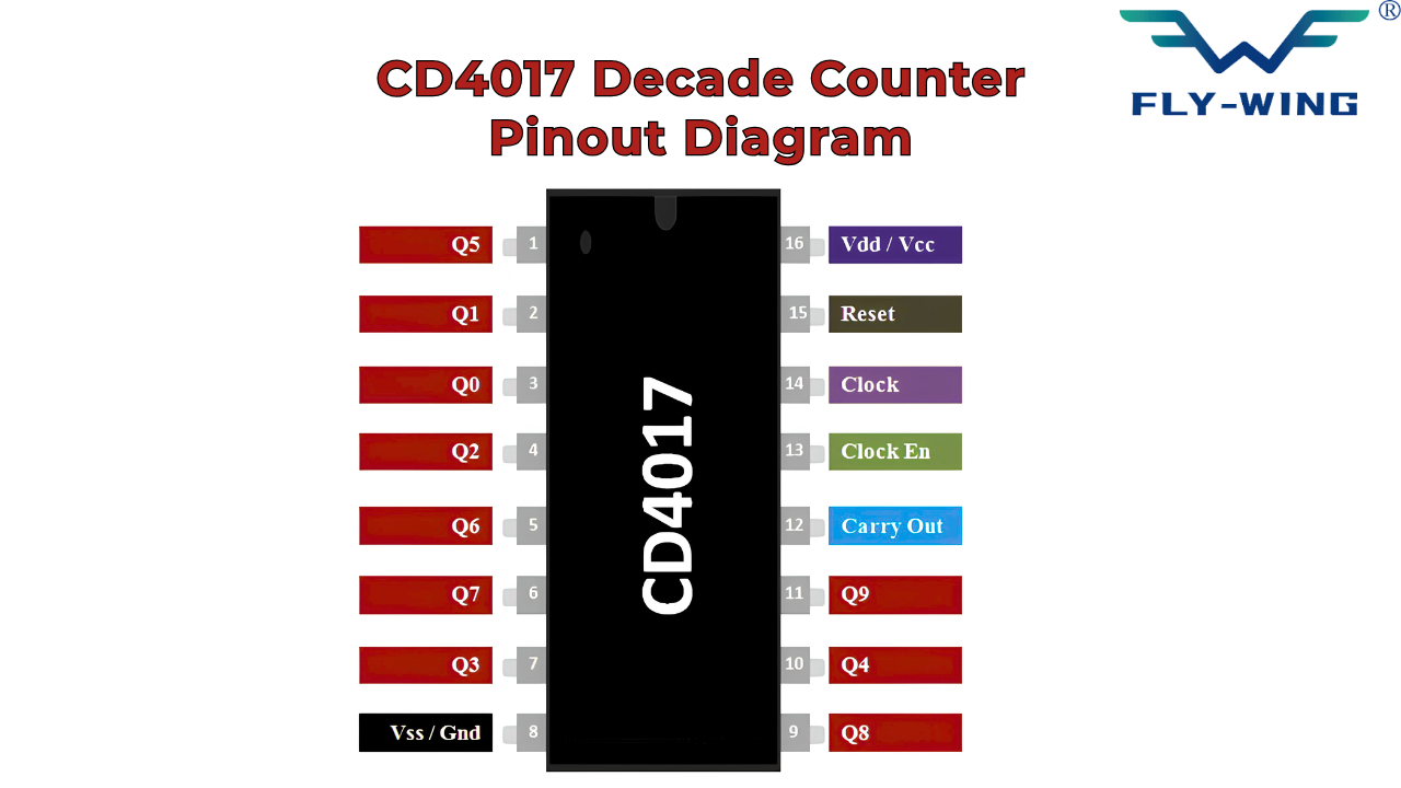
| Pin | Name | Function |
|---|---|---|
| 1 | GND | Ground — system reference (note: some sources label pin 8 as GND; verify against your specific datasheet revision) |
| 2 | Q5 | Decoded output 5 — goes HIGH on the 6th clock pulse |
| 3 | Q0 | Decoded output 0 — first output, HIGH at startup/reset |
| 4 | Q1 | Decoded output 1 — HIGH on the 2nd clock pulse |
| 5 | Q2 | Decoded output 2 — HIGH on the 3rd clock pulse |
| 6 | Q6 | Decoded output 6 — HIGH on the 7th clock pulse |
| 7 | Q7 | Decoded output 7 — HIGH on the 8th clock pulse |
| 8 | GND / VSS | Ground connection — negative supply reference |
| 9 | Q8 | Decoded output 8 — HIGH on the 9th clock pulse |
| 10 | Q4 | Decoded output 4 — HIGH on the 5th clock pulse |
| 11 | Q9 | Decoded output 9 — HIGH on the 10th clock pulse |
| 12 | CO | Carry Out — goes HIGH after every 10 clock pulses, used for cascading |
| 13 | CE | Clock Enable — active-HIGH inhibit; tie LOW for normal counting |
| 14 | CLK | Clock input — Schmitt-triggered, advances count on rising edge |
| 15 | MR / RESET | Master Reset — active-HIGH; forces counter back to Q0 |
| 16 | VDD | Positive supply voltage (3 V to 15 V) |
The Non-Sequential Output Layout — A Common Source of Wiring Mistakes
One thing that surprises many new builders about the IC packaging is that the output pins are not ordered in sequentially numbered around the package. Although pin 3 has Q0, 2 has Q1, and 4 has Q2, there is no sequential numbering because of the way the internal Johnson counter and Decoder Logic route to the physical connections.
This is not an error in documentation; it was the way the chip was designed, and all legitimate datasheets will show the same non-sequential mapping for output pins. The solution is to always wire by output function (Q0, Q1, Q2…) using the pin reference table, and do not assume the pin labels increase sequentially around the package.
Clock Input and Clock Enable
Pin 14 is the Clock input; it produces a rising edge output on the rising edge of the clock signal from LOW to HIGH; therefore, each rising edge of the Clock signal advances the Count by one count. The Clock Enable pin (Pin 13) will only count the Clock signal in these two states (HIGH means it will count), and when it is an active LOW, it will ignore all clock signals and hold its state. To allow for normal continuous counting, connect the Clock Enable to the ground.
Reset and Carry Out
Pin 15 is Master Reset; also denoted as MR; when the Master Reset pin is pulled to a HIGH, the counter will be forced to Q0. This occurs regardless of the clock’s state. For normal operation, connect the M Reset to the Ground. Pin 12 is the Carry-Out (CO); the CO pin will be HIGH during the second half of every 10 counts (5-9) and will be LOW during the first half. The CO pin of the counter completes one full cycle (HIGH and LOW) during the 10 clocks, i.e., it is the correct signal to cascade to the second CD4017.
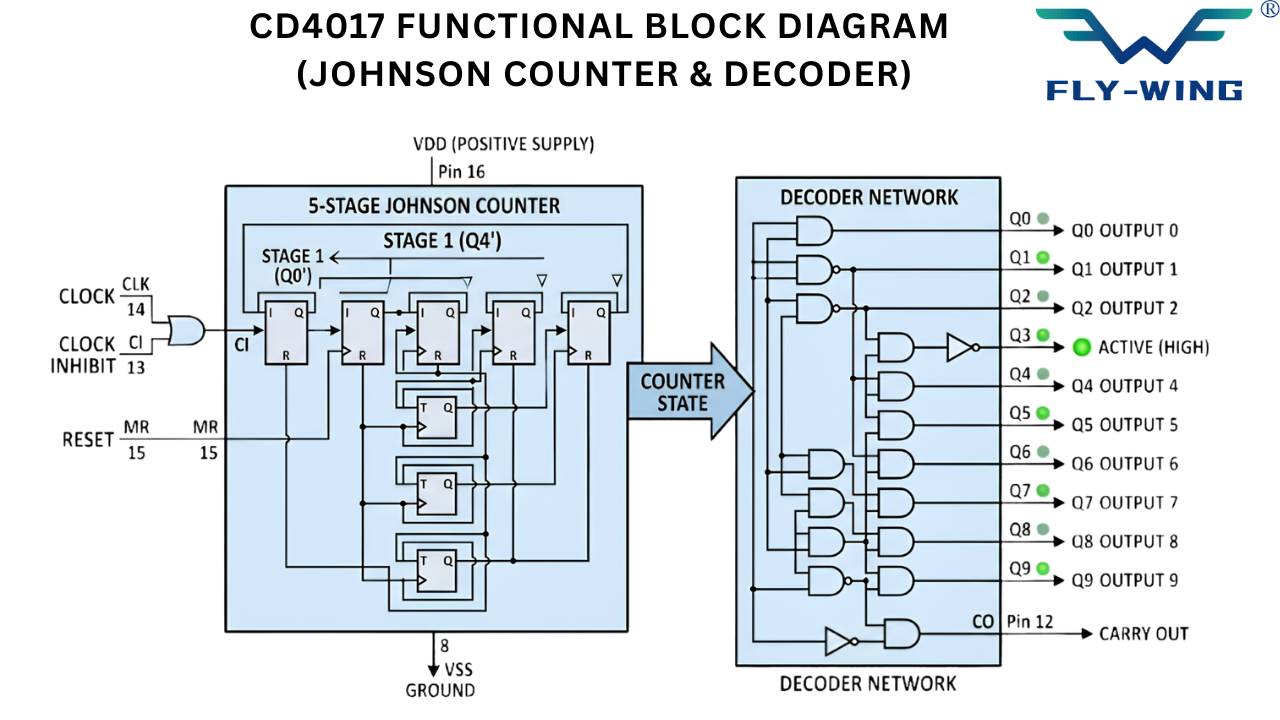
How the CD4017 Works Internally: Johnson Counter and Decoder
Understanding the internal logic removes the mystery and makes every external wiring decision make sense.
The Johnson Counter Core
The core of the CD4017 is a chain of five D-type flip flops in the form of a ring, which is also known as the Johnson counter (switch-tail ring counter). The output from one flip-flop is fed to the next, with the inverted output of the fifth flip-flop returned to the first flip flop. A Johnson counter has 10 unique internal states for every 10 pulses applied to its input, despite having five flip flops.
A typical chain of five flip flops can generate 32 different binary states (2^5). But in the case of the Johnson counter, out of the total 32 states only 10 states are utilized. It has been done intentionally because of the sequence in which the states are generated. Such a sequence makes it possible to generate a very simple decoder for the 10 states.
The Decoder Stage: Converting Internal States to One-Hot Outputs
The decoder circuitry, made up of a combination of inverters and logic gates, checks the five flip-flop statuses and ensures that only one of the ten Q outputs is on at a time. In this case, we say there is one-hot encoding because only one output is on (HIGH) at a time, while all other output lines remain off (LOW).
The above scenario is completely different from a binary counter. For example, a 4-bit binary counter has the number 5 encoded as 0101; that is, two output lines are HIGH while two are LOW. This requires additional decoding to have one indicator line. However, in CD4017, 5 is represented when the pin Q5 goes HIGH.
Count Sequence and Rollover
The typical start-up condition of the CD4017 is that the output Q0 will be HIGH when the device powers up (even though this is not always true; it may sometimes require an initial reset pulse to assure this start-up condition), and on each successive positive-going clock pulse, the HIGH output shifts to the next pin in order: Q0 -> Q1 -> Q2 -> … -> Q9. Once Q9 has become HIGH and another clock pulse occurs, the device resets back to Q0, and the process begins again.
Always use a clean oscillator source (like a 555 timer) or proper hardware/software debouncing for switch-based clock inputs.
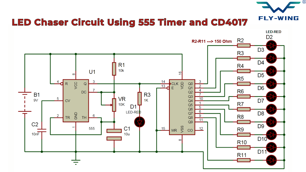
Building a CD4017 LED Chaser Circuit with a 555 Timer
This is the canonical CD4017 project, and for good reason. It demonstrates every core concept of the chip in a circuit you can build on a breadboard in under twenty minutes.
Why Pair the CD4017 with a 555 Timer
In order for the CD4017 to count correctly, it will require an external source of clock pulses (due to the lack of a built-in clock generator). The easiest and most reliable method of generating that clock pulse is by using a 555 timer configured in the “astable” mode. This configuration will produce a continuous square wave with a frequency that is determined by two resistors and a capacitor that can be easily calculated and adjusted, but will still tolerate any wiring imperfections associated with using a breadboard.
Component List
- CD4017 decade counter IC (16-pin DIP)
- NE555 timer IC (8-pin DIP)
- 10 LEDs (any color, standard 5mm)
- 10 × 220Ω resistors (current limiting — one per LED)
- R1: 10kΩ resistor (555 timing)
- RV1: 50kΩ potentiometer (555 timing — speed control)
- C1: 10µF capacitor (555 timing)
- C2: 0.01µF capacitor (555 control voltage filtering, pin 5)
- 0.1µF decoupling capacitors × 2 (one near each IC’s power pins)
- 9V battery or regulated power supply
Wiring the 555 Timer (Astable Mode)
- Pin 8 (VCC) → positive supply rail
- Pin 1 (GND) → ground rail
- Pin 4 (Reset) → tied directly to VCC (prevents accidental reset)
- Pin 5 (Control Voltage) → 0.01µF capacitor to ground (noise filtering, not used for control here)
- Pins 6 and 7 → connected together, through R1 and RV1 in series to VCC
- Pin 2 → connected to the junction of pins 6/7 (discharge path) and to C1, which connects to ground
- Pin 3 (Output) → this is the clock signal — connect to CD4017 pin 14
Wiring the CD4017
- Pin 16 (VDD) → positive supply rail
- Pin 8 (GND) → ground rail
- Pin 14 (CLK) → 555 timer pin 3 (clock signal in)
- Pin 13 (CE) → ground (enables continuous counting)
- Pin 15 (MR/Reset) → ground (disables reset, allows free counting)
- Pins for Q0–Q9 → each through its own 220Ω resistor to the anode of an LED; LED cathodes to ground
Adjusting Chase Speed
The 555 timer’s oscillation frequency is determined by a potentiometer (RV1). This will directly influence how quickly the LED light sequence changes. With the maximum resistance (approximately 50k), the oscillation is approximately 0.7Hz (slow). With RV1 at the minimum resistance (approximately 1k), the oscillation is running at around 7Hz (quick and blurry). At 25k, the oscillation is approximately 1.4Hz, which should be suitable for a majority of decorative uses.
The working principle is simple: as resistance decreases, the time for C1 to charge and discharge is reduced, which increases the frequency of oscillation and therefore the rate at which the LEDs will change. If you know how fast you want the LEDs to “chase,” you can calculate the 555 astable frequency formula first, then choose the component values to give you the desired output.
Advanced CD4017 Circuits: Cascading and Frequency Division
6.1 Cascading Multiple CD4017 ICs
If more than ten outputs are required, for example, twenty LEDs chasing in sequence, you can use two CD4017 chips in cascade. To do this, connect the Carry Out pin of the first chip (pin 12) to the Clock In pin of the second chip (pin 14). The first chip will count normally through its Q0 to Q9 outputs, but every time there is a complete cycle of ten counts in the first chip, the Carry Out pin will transition high, creating one clock pulse for the second chip.
As a result, every time the first chip has completed a ten-count cycle, the second chip moves to the next LED. By connecting all the outputs of both chips to sequentially lit LEDs, you will have a cascading chase with twenty LEDs. You can continue this pattern for thirty, forty, or even more outputs by connecting additional CD4017s using the above process.

Divide-by-N Frequency Division
The CD4017 also works as a programmable frequency divider for all integers from 2 to 9. You can do this by connecting the reset pin (pin 15) to the output pin that is associated with the integer you want to divide by.
As an example, if you wanted to create a divide-by-9 circuit, you would connect Q9 (the 10th output; pin 11) to the reset pin (pin 15). As the counter counts through Q0 – Q8, when Q9 would normally go low, it instead goes low, immediately resetting the counter back to Q0. Therefore, the total number of counts is 9 instead of 10; you have divided the frequency of the incoming clock signal by 9.
- Divide by 2: connect Q2 (pin 4) to Reset — counter cycles through Q0, Q1 only
- Divide by 5: connect Q5 (pin 2) to Reset — counter cycles through Q0–Q4
- Divide by 7: connect Q7 (pin 7) to Reset — counter cycles through Q0–Q6
- Divide by 9: connect Q9 (pin 11) to Reset — counter cycles through Q0–Q8
Noise Immunity on Control Pins
Reset and Clock Enable lines are CMOS high-impedance inputs. If left floating (not connected), these lines become very prone to picking up electrical noise from surrounding switching circuits or even the ambient fluorescent lights. A floating Reset line may randomly go active, resetting your counter at some random point during the sequence.
The fix: Always keep Reset and Clock Enable lines tied down. If the line must be LOW when your circuit is operating normally, tie it to ground; otherwise, pull it down using a resistor (commonly 10 kilo-ohms) if the line should sometimes be HIGH due to some other part of the circuit.
CD4017 vs. 74HC4017 vs. Arduino-Based Counters
The CD4017 is not the only way to build a sequential output circuit. Choosing between it and the alternatives depends on your speed requirements, power budget, and how much flexibility your project needs.
| Parameter | CD4017 | 74HC4017 | HEF4017 | Arduino-based |
|---|---|---|---|---|
| Logic Family | CMOS (4000B) | HCMOS | CMOS | Microcontroller |
| Voltage Range | 3–15 V | 2–6 V | 3–15 V (to 18V) | 5 V (typical board) |
| Max Frequency | ~10 MHz | ~50 MHz | ~12 MHz | Software-limited |
| Static Power | Microwatt | Microwatt | Microwatt | Milliwatt+ (MCU active) |
| Pattern Flexibility | Fixed sequence | Fixed sequence | Fixed sequence | Fully programmable |
| Component Count | Low (IC + clock) | Low (IC + clock) | Low (IC + clock) | MCU + code, fewer discretes |
| Best For | Simple hobby/edu circuits | Faster digital systems | Industrial wide-voltage | Custom or complex patterns |
CD4017 vs. 74HC4017: Logic Family Differences
The 74HC4017 is identical to CD4017 in terms of pinout and counting functions, but it is made in HCMOS (High Speed CMOS) technology and not the 4000B series CMOS technology. The key differences: 74HC4017 operates in a narrower range of operating voltage (about 2-6 volts, better suited for modern 3.3v/5v systems) but reaches much higher max frequency — typically about 50 MHz, as opposed to 10 MHz in the case of CD4017.
As far as LED chaser and other timing circuit projects go, this difference does not matter in practice — both ICs work at frequencies that are orders of magnitude higher than those used in these circuits. CD4017 offers better flexibility in battery-operated projects due to a wider input voltage range.
When a Microcontroller Makes More Sense
An Arduino or similar microcontroller can replicate the CD4017’s sequencing behavior in a handful of lines of code, driving any number of outputs in any custom pattern — not just a fixed one-direction sequence. If your project needs the chase to reverse direction, skip outputs in a non-sequential pattern, or respond to sensor input, a microcontroller offers far more flexibility than hardware logic ever could.
The trade-off is complexity and cost. A CD4017 plus a 555 timer costs less than a dollar in components and requires no code. An Arduino Uno costs significantly more and requires writing, uploading, and debugging firmware. For a fixed, simple, one-direction LED chase, the CD4017 approach remains genuinely simpler — not just nostalgic.
Equivalent and Pin-Compatible Parts
Different manufacturers produce the same functional part (with different names). The functionality and pinout configuration of the HEF4017 (from NXP/Philips), MC14017 (from Motorola/ON Semiconductor), and CD4017 are identical; however, the electrical specifications (Input Voltage Range & Max Frequency) may vary slightly between the various manufacturers, so you must check the manufacturer’s specific datasheet for the exact voltage range and maximum frequency before substituting any of these components.
Troubleshooting Common CD4017 Problems
LEDs Not Chasing at All
First, check if the Clock Enable pin (13) is accidentally high? If this happens, then the IC does not respond to any clock pulse and retains its present output. Make sure it is grounded. Second, check whether there is any clock pulse available at pin 14? Use a multimeter or LED indicator at the output of the 555 timer (pin 3) to confirm the same. Third, check whether the reset pin (15) is high and is holding the counter output at Q0?
Random Flickering or Skipped Counts
It indicates that there must be clock signal noise or fluctuation in the power supply. In order to resolve the problem, add 0.1µF decoupling capacitors between the VDD and GND pins of both the CD4017 and 555 timer, as close as possible to the IC pins. Transitions due to the switching noise in the power line, without proper decoupling, can trigger unwanted transitions in the clock line.
If clock signals are triggered from the mechanical switch rather than the 555 timer, then the reason may be the switch bounce. It means that pressing of a single physical switch results in multiple transitions of the electrical signal because the contacts bounce back and forth a number of times. Thus, a debounce mechanism should be added to the clock line.
Speed Control Not Working
In case there is no effect on the speed of chasing by turning the potentiometer, three items must be checked: the potentiometer is wired as a variable resistor in series with the 555 timing circuit (not wired as a voltage divider to feed an unrelated pin), the capacitor C1 in the 555 timing circuit is not open or shorted, and the potentiometer is not faulty.
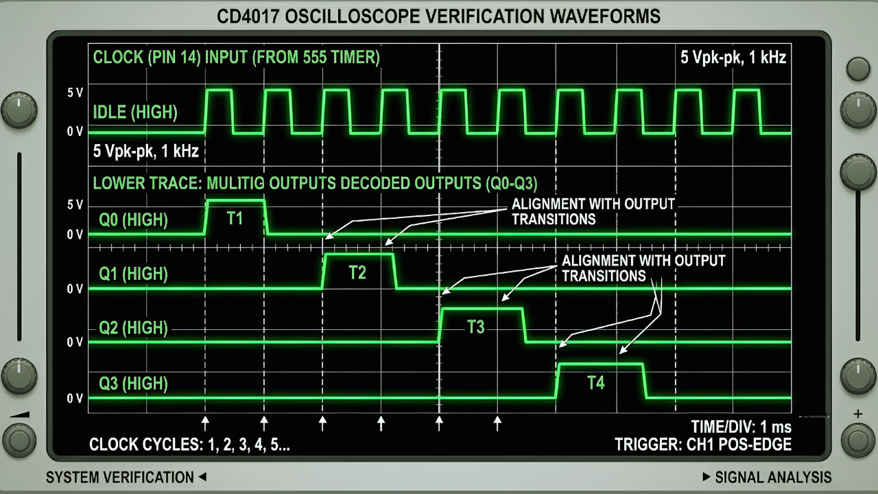
Oscilloscope Verification
First, use the probe to test pin 14 (Clock). When the probe touches pin 14, you should see a sharp-edged square wave output at the frequency you have established by adjusting the RC network of the 555 timer. If there is either rounding of the square wave or multiple fast transitions near the edges of the square wave, then you have a problem with noise or excessive loading due to the upstream devices connected to pin 14.
Next, test the output pins from Q0 to Q9 in order, or if you are lucky enough to have a multi-channel oscilloscope, test all of the output pins at the same time by connecting each output pin to its dedicated channel. When testing the outputs, you should see a clean LOW-to-HIGH transition at the output pin for one clock cycle. After one clock cycle, the output should return to a LOW state so the next output pin can be driven HIGH. If any output stays HIGH for more than one clock cycle, or fails to drive HIGH, there is a problem with the wiring to that output pin.
Frequently Asked Questions
The CD4017 is a CMOS decade counter and decoder IC that counts clock pulses from 0 to 9 and activates one output (Q0–Q9) at a time in sequence. It is commonly used in LED chasers, sequencers, and frequency divider circuits.
The CD4017 can operate at approximately 10 MHz, depending on the supply voltage. At lower voltages, the maximum frequency decreases, but this is rarely a limitation for LED chaser circuits, which typically run below 100 Hz.
Yes. Connect the Carry Out pin (12) of one CD4017 to the Clock input (14) of the next. Each additional IC adds 10 sequential outputs, allowing two ICs for 20 outputs, three for 30, and so on.
Connect the required output pin to the Reset pin (15). For example, connecting Q9 to Reset creates a divide-by-9 counter by resetting the IC before Q9 becomes active.
Both ICs have the same pinout and counting function. The CD4017 uses standard CMOS technology with a wider voltage range (3–15 V), while the 74HC4017 uses HCMOS technology with a lower voltage range (2–6 V) and higher speed capability. Both are suitable for LED chaser projects.
This is normal. The output pins are not arranged sequentially on the package; for example, Q0 is pin 3, while Q1 is pin 2 and Q2 is pin 4. Always follow the output labels (Q0, Q1, etc.) rather than the physical pin order.
Conclusion
The CD4017 decade counter integrated circuit is one of the easiest and most effective ways to design sequential output circuits. This device combines a Johnson counter and decoder in a single package, allowing it to generate 10 sequential outputs from a clock signal without requiring additional decoding circuitry or programming. Its wide operating voltage range, low power consumption, and simple operation make it a popular choice for LED chasers, frequency dividers, educational projects, and basic automation systems.
In this guide, we covered the CD4017 pinout, electrical specifications, internal Johnson counter architecture, working principle, LED chaser circuit design using a 555 timer, cascading techniques for additional outputs, frequency division applications, troubleshooting methods, and comparisons with alternative solutions such as the 74HC4017 and Arduino-based counters.
Whether you are building a simple LED chaser, expanding output channels with multiple CD4017s, or creating a reliable frequency divider, the CD4017 remains a cost-effective and dependable solution. By understanding its operation and design considerations, you can confidently use this versatile IC in a wide range of digital electronics projects.
COMMENTS