Introduction
In the power electronics design, choice of the MOSFET is one of the most critical decisions. An inappropriate choice of MOSFET can result in significant power dissipation and thermal stress, compromising efficiency and eventually leading to catastrophic system failure. In contrast, an optimised selection enhances power density and thermal headroom ensuring long term reliability.
MOSFETs play a vital role in switching and control of many modern applications i.e., DC-DC converters, Battery Management Systems (BMS), motor drives, inverters, etc. Given the thousands of devices available on the market, selecting the one requires the clear understanding of key parameters and application requirements. This guide demonstrates a practical engineering approach to the MOSFET selection, giving you the insight to choose components that hold up to the physical stresses and thermal realities of your actual design.
What is MOSFET?
Fundamentally, a MOSFET (Metal-Oxide-Semiconductor Field-Effect Transistor) is voltage-controlled switch used for high-speed switching and power control. Fig-1 shows a cross-sectional view and circuit symbol of MOSFET. In power electronics, MOSFETs are primarily used as:
- High-speed Switches
- Low conduction losses
- Ease of gate drive
The main applications are:
- DC-DC converters
- Power inverters
- Motor drives
- Battery management systems
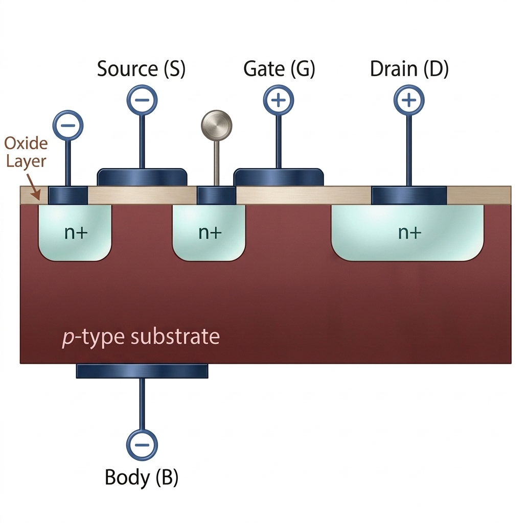
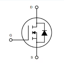
Fig-1: Cross-sectional view of MOSFET (Left Figure) and power MOSFET symbol (Right Figure)
Key Parameters for MOSFET Selection
Selecting an appropriate MOSFET for your system requires evaluating various critical parameters. Missing even one critical parameter can introduce design inefficiencies or cause complete circuit failure.
Drain-Source Voltage (Vds)
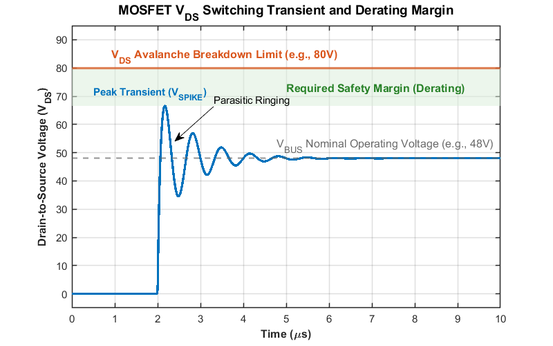
This parameter refers to the maximum voltage that MOSFET can withstand between drain and source without damaging itself.
Standard Engineering Practice: For your design, choose the MOSFET with
\[V_{ds} \ge 1.2 \times \text{maximum system voltage}\]
As shown in Fig-2, system transients and dv/dt spike pushes the voltages well beyond the nominal levels. Hence, selecting a MOSFET with adequate margin prevents breakdown.
Continuous Drain Current (Id)
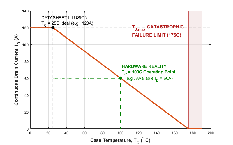
Drain current (Id) defines the absolute maximum current a MOSFET can sustain before thermal failure. While this parameter is prominently listed on page one of datasheet, relying solely on this nominal value is dangerous. Manufacturers specify this limit assuming an idealised temperature of 25°C. However, in practical designs thermal derating should be considered (see Fig-3).
On-State Resistance (Rds(on))
This is the resistance between drain and source when MOSFET is conducting. This parameter is very important as it dictates the conduction losses in the system. The conduction losses are defined as:
\[P = I^2R\]
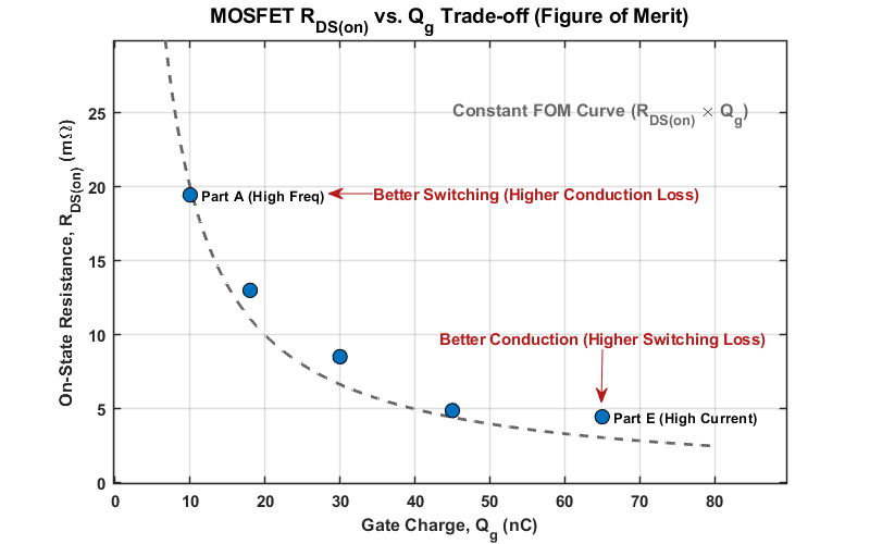
While it is tempting to select a device with lowest Rds(on), however one must navigate a critical design trade-off:
- Lower Rds(on) reduces the power dissipation, so the conduction losses are reduced.
- However, Achieving a lower Rds(on) requires a larger silicon die area, which inherently increases parasitic gate charge (Qg) leading to higher switching losses.
To find the optimal balance, engineers evaluate the MOSFET ‘s Figure of Merit (See Fig-4)
\[FOM = R_{DS(on)} \times Q_g\]
Gate Charge(Qg)
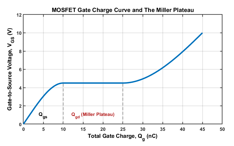
Gate charge determines the energy required to switch the MOSFET on and off. This effects the transition speed and dynamic losses such as, higher Qg leads to higher switching losses and will require a more robust gate driver, while lower Qg is essential for maintaining efficiency specially in high frequency operations.
To visualize this, Fig-5 demonstrates the typical gate charge curve. The flat section is knowns as the miller plateau (Qgd) and it is the exact moment the MOSFET transitions between on and off, making it the primary source of switching losses.
Design Factors and Impact on MOSFET Performance
In real designs, MOSFET performance is not determined solely by datasheet parameters. Various other factors such as switching frequency, thermal conditions, gate driver capabilities, etc. influence the real-world behaviour. The table below highlights the key factors and their impact on system level performance.
| Design Factors | Affected Parameters | Impact on Performance |
| Switching frequency | Qg , switching losses | Higher switching losses |
| Load current | Rds(on), Id | Higher conduction losses |
| Ambient temperature | Rds(on), Id | Possible device destruction |
| Gate drive strength | Qg , switching speed | Slower switching hence more losses |
| PCB layout | Switching behaviour | Ringing and EMI issues |
| Cooling conditions | Thermal resistance ( Rth) | Improves power handling |
Step-by-Step MOSFET Selection Guide for Power Electronics Design
Step-1: Identifying Application Requirements
The first step is to always establish the absolute boundary conditions of your design, specifically:
- Input voltage
- Output voltage
- Maximum peak current
- Operating frequency
- Ambient temperature range
Step-2: Choose Voltage Ratings (Vds)
As discussed earlier, to prevent catastrophic failure due to inductive spikes and switching transients, the Vds must be 20-30% higher than the maximum voltage of your design.
\[V_{ds} \ge 1.2 \times \text{maximum system voltage}\]
Step-3: Current Handling in MOSFETs and Derating with Temperature
The next step is to identify the current rating of the MOSFET. It is critical design error to rely on the maximum current value printed on the first page of datasheet. In real world applications, the current ratings derate with the temperature rise. Hence, it is important to analyse how the current capability of MOSFET decreases based on:
- Case temperature and Heatsinking
- Junction temperature
- Airflow
Step-4: Losses Evaluation in MOSFETs
Evaluating power losses is a critical step before selecting the MOSFET because it dictates that thermal management and system efficiency. There are mainly two types of losses in MOSFET i.e. switching and conduction losses. To optimize your design, the following parameters should be balanced based on following parameters:
- Lower Rds(on): To minimize conduction losses under heavy load currents
- Acceptable gate charge (depends on operating frequency): Directly impact on switching losses
Step-5: Calculating Temperature Rise
The final step is verifying that designed PCB and cooling strategies can keep the temperature of silicon die under the maximum temperature ratings. The temperature rise can be calculated using the formula given below:
\[T_j = T_a + (P_d \times R_{\theta JA})\]
Here,
- Tj=Junction temperature
- Ta=Ambient temperature
- Pd=Total losses
- RθJA=Junction to ambient thermal resistance (found in datasheet)
Practical Example for the Selection of MOSFET
This section demonstrates a practical example of selecting a suitable MOSFET in the real power electronics design based on the aforementioned procedure.
Step-1: Defining System Requirements
Assuming a MOSFET selection for a DC-DC converter used in industrial or telecom applications. The system parameters are given as follows.
| Parameter | Value |
| Input voltage | 36V-60V |
| Nominal voltage | 48V |
| Output power | 500W |
| Switching frequency | 100kHz |
| Ambient temperature | 40°C |
Step-2: Choose Voltage Ratings (Vds)
Considering the safety margin for switching transients
\[V_{ds} \ge 1.2 \times 60 = 72\text{V}\]
So, MOSFET with Vds greater than 72V will be standard choice for the specific application.
Step-3: Current Requirements of MOSFET
For a 500W system with nominal voltage of 48V, the current drawn by load is 10.4A. As the junction temperature rises, MOSFET’s current handling capability drops. To guarantee, long term reliability, it is advisable to apply a 2x to 3x safety multiplier. Hence, Id greater than 20-30A will be suitable for this application.
Step-4: Losses Evaluation of MOSFET
Assuming the Rds(on) of 4mΩ, the conduction losses will be 0.4W. Assuming the Qg of 38nC with rise time (tr) and fall time (tf) of 15ns, and switching frequency of 100kHz the switching losses will be 0.72W leading to total losses of 1.12W.
Step-5: Calculating Temperature Rise
Thermal rise of the MOSFET is dependent on total losses and thermal resistance. Here, we consider three different cases.
- Case-1: Basic PCB without heatsink (RθJA= 40°C/W)
- Case-2: Good PCB with thermal vias and wide copper (RθJA= 25°C/W)
- Case-3: PCB with better cooling (RθJA= 15°C/W)
The table below presents a direct comparison of these three cooling strategies.
| Condition | Thermal Resistance | Power Loss | Temperature Rise | Junction Temperature |
| Basic PCB | 40°C/W | 1.16W | 46.4°C | 86.4°C |
| Good PCB | 25°C/W | 1.16W | 29°C | 69°C |
| With Cooling | 15°C/W | 1.16W | 17.4°C | 57.4°C |
By following these design steps, we have clearly defined exact parameters required for our specific application. The parameters are summarized in table below.
| Parameter | Final Requirement |
| Vds | ≥ 100V |
| Id | ≥ 20A |
| Rds(on) | ≤ 8–10 mΩ |
| Qg | ≤ 40 nC |
| Thermal Resistance | ≤ 25–30 °C/W |
MOSFET Recommendation for 48V DC-DC Converter
Based on the estimated system parameters for this 48V, 500W, and 100kHz system, the Infineon BSC098N10NS5ATMA1 is the optimal choice. Along with Vds and Id requirements, it perfectly balances the lower Rds(on) and has a lower Qg of 22nC which insures maximum power efficiency and thermal reliability. If your supply chain requires alternative sourcing, or if your thermal constraints vary slightly, the Alpha & Omega AON6294 serves as another excellent 100V N-Channel alternative that offers competitive switching characteristics and thermal

Common Mistakes to Avoid During MOSFET Selection
Selecting a MOSFET is not about comparing datasheet values. It requires system level understanding of electrical, thermal, and switching requirement of the device. Even a experienced engineers can make a mistake leading to overheating, reduced efficiency or device failure. Following are the most common mistakes and how to avoid them.
Ignoring thermal limits and Real Operating Conditions
One of the most common mistakes is understanding thermal limits. While MOSFET may appear suitable based on voltage and current ratings, excessive power dissipation can cause higher junction temperatures leading to device failure
In practical applications, MOSFET does not operate under ideal conditions. Factors such as ambient temperature, PCB layout, and airflow significantly affect thermal performance. For example, even a small increase in power loss (1-2W) can double the temperature rise (based on thermal resistance). This can push the junction temperature beyond the safe operating limits
How to Avoid
The best practice is to always calculate losses and evaluate junction temperature using realistic thermal values. In practice, engineers include safety margins to ensure long term reliability.
Overlooking Gate Drive Requirements
Another critical but often overlooked factor is gate drive capability. A MOSFET is not passive component, it requires proper driver to operate efficiently. If gate driver can not supply sufficient current, MOSFET will switch slowly. This will enhance the switching losses particularly in high-frequency applications such as DC-DC converters, inverters, etc.
How to Avoid
It is necessary to ensure that the gate driver:
- Provides sufficient voltage (8-15V for standard MOSFETS)
- Has adequate capacity to charge and discharge gate capacitors
- Matches the switching frequency requirement of the system
Ignoring Switching Frequency Impact
Switching frequency plays a vital role in the selection of MOSFET for power electronics design. At lower switching frequency conduction losses dominate, however as the switching frequency increases, switching losses become significant.
Designers sometimes select the MOSFET optimized for lower frequency and use it for higher frequency operations which lead to excessive heating and poor efficiency.
How to Avoid
- For lower frequency operation prioritize Rds(on).
- For high frequency systems focus on lower gate charge and switching speeds
Not Considering Safe Operating Area (SOA)
Safe Operating Area (SOA) defines the limits of MOSFET within which MOSFET can operates without damage. Ignoring SOA will result in device failure, especially in applications such as motor drives, grid-connected inverters where switching transients impose severe impact on the system performance.
How to Avoid
In order to avoid this issue, it is important to verify that MOSFET operates within SOA under all the conditions such as transients, fault conditions, etc.
Applications of MOSFETs
MOSFET Selection for Different Applications
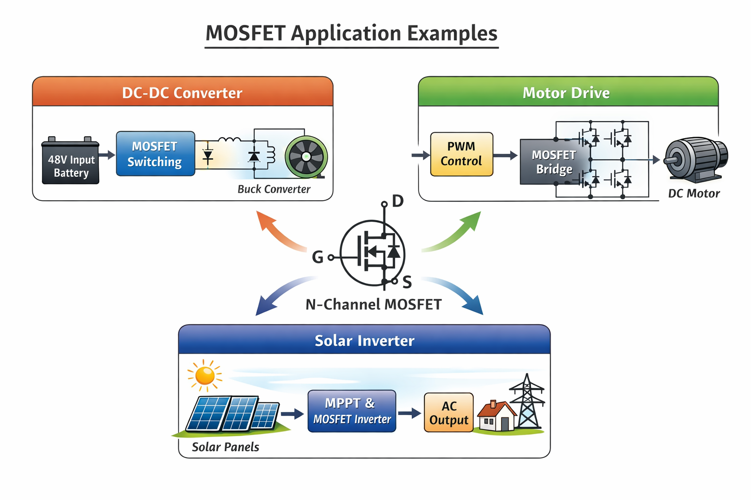
While every parameter discussed is critical, different applications require different design priorities. The table below highlights the critical MOSFET parameters priorities based on the different applications.
| Application | Key Focus | Example Needs |
| DC‑DC Converter | Low Rds(on), low Qg | High efficiency at high frequency |
| Motor Drive | High current, robust | Thermal capability |
| Inverter | High voltage, fast switching | Balanced switching characteristics |
Conclusions
Choice of appropriate MOSFET is a critical step in designing a reliable and efficient power electronics design. A proper design methodology involves several steps such as understanding system requirements, analyzing switching and conduction losses, performing thermal analysis to ensure safe operation, and considering driver requirements, etc.
In real-world designs, trade-offs are bound to happen. Such as, a MOSFET optimized for lower conduction losses may not perform better with higher switching frequency, while a fast-switching MOSFET may introduce higher conduction losses. Hence, the goal is not to find the best MOSFET in general, but the most suitable one for the specific power electronics application.
For example, as discussed earlier, selecting low Rds(on), 100V MOSFET reduces conduction losses significantly and maintains the junction temperature within the safe operating limits. This justifies how a proper selection of switching device directly impacts the reliability, thermal performance and efficiency of system.
To conclude, by following structured and analytical approach given in this guide, engineers can select an appropriate MOSFET for their power electronics design and can avoid the common mistakes in the design process.
Frequently Asked Questions (FAQs)
Standard engineering practice dictates that the Drain-to-Source Voltage ($V_{DS}$) rating should be at least 20% higher than your maximum system voltage. For example, in a 60V system, you should select a MOSFET with a $V_{DS}$ of at least 72V ($V_{DS} \ge 1.2 \times 60\text{V}$) to safely handle voltage spikes and transients.
The primary trade-off in MOSFET design is between conduction losses and switching losses. To achieve a very low On-resistance ($R_{DS(on)}$), the physical silicon die must be larger, which inherently increases the internal capacitance and total gate charge ($Q_g$). You must balance these two parameters based on your switching frequency.
A MOSFET’s ability to handle continuous current drops significantly as its junction temperature increases. If you select a component rated exactly for your nominal current at room temperature, it will likely overheat and fail under real-world loads. Designers typically apply a 2x to 3x safety multiplier to the continuous drain current ($I_D$) rating to account for thermal derating.
The Figure of Merit (FOM) is an industry metric used to evaluate a MOSFET’s overall efficiency, calculated by multiplying its On-resistance by its gate charge ($FOM = R_{DS(on)} \times Q_g$). A lower FOM indicates a better-optimized device that effectively balances static conduction efficiency with dynamic switching performance.
Yes, but it depends heavily on your total power dissipation ($P_d$) and your PCB layout. If your static and dynamic losses are low, an optimized PCB with thermal vias and wide copper pours can keep the Junction-to-Ambient thermal resistance ($R_{\theta JA}$) low enough to safely dissipate the heat without an external heatsink.