Introduction
In modern digital systems, high-speed memory has become a critical performance parameter, and Dual Data Rate (DDR) memory modules, such as DDR3, DDR4, and LPDDR4, offer large storage capacity with high bandwidth and performance. Interfacing the DDR4 memory with the FPGA is a challenging task that requires both knowledge and technical expertise, as incorrect interfacing can impact speed and stability.
In modern digital systems, such as embedded systems and real-time signal processing, DDR memory and its interfacing with an FPGA are core requirements of SoC designs. It is therefore, interfacing the DDR with the FPGA requires a solid grip on high-speed signal integrity, controller configuration, and power supply requirements.
This technical tutorial provides a comprehensive hardware-level guide that fills the gap between theory and real-world implementation. This tutorial will help you understand by a step-by-step guide on how to interface DDR memory modules in FPGA and SoC design. At the end of this tutorial, you will be able to interface or implement DDR memory with an FPGA.

Understanding DDR Memory Basics
Before we move into the topic of interfacing DDR memory with FPGA, it is important to understand the basics of DDR memory and how it works, its principle, and what are some of the types of DDR memory. DDR stands for Double Data Rate because it transfers data on both rising and falling edges of the clock signal. This prime feature of DDR makes it ideal for high-speed applications, including AI accelerators, real-time signal processing, and modern embedded system applications.
What is Memory and Its Types
Memory devices are nothing but storage devices that store data/information in electronic products such as computers. Their primary purpose is to store the processed data and ensure that it is available when the controller requires it. On a broader level, the memory devices are categorized into two main types, namely primary memory and secondary memory.
The primary memory is further categorized into Random Access Memory (RAM) and Read-Only Memory (ROM). The difference between RAM and ROM is that RAM is volatile memory, i.e., data is lost after the power is switched off. However, the ROM is non-volatile memory, i.e., it retains the data even when the power is switched off. The further classification is shown in the figure below.
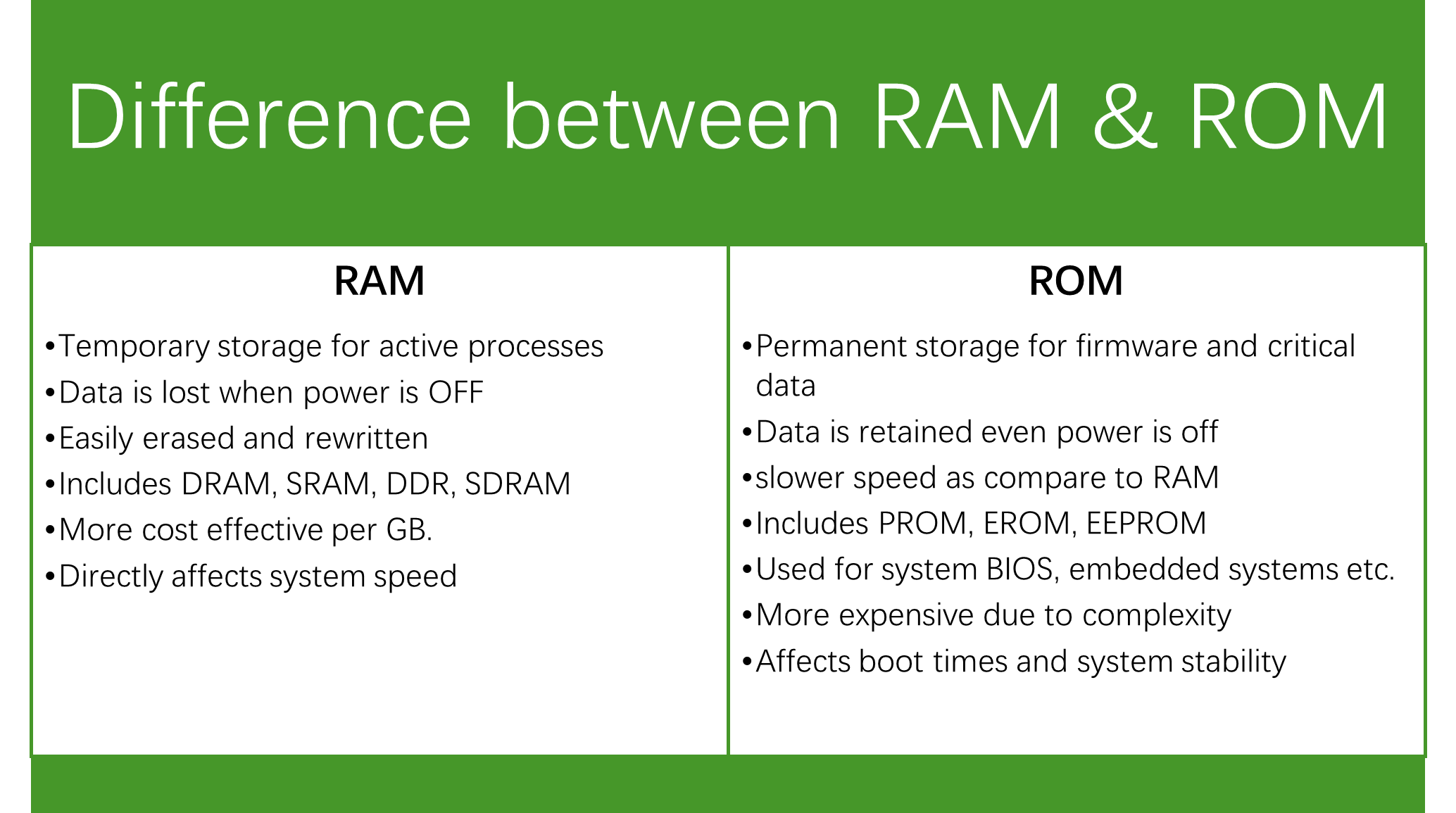
The primary memory includes the DRAM, SRAM, DDR, and SDRAM. All these are types of RAM but with different architectures. The SRAM is the static RAM, and its architecture consists of one flip-flop to store one bit; the DRAM is dynamic RAM, and its architecture consists of one transistor and one capacitor for one bit memory. The SDRAM is synchronous dynamic RAM, and its architecture is the same as DRAM, i.e., it requires 1 transistor and a capacitor for one bit of memory. However, the SDRAM is a faster and clock-synchronized version of DRAM that allows parallel operations.
SRAM is faster because it uses flipflop and therefore does not need refreshing like DRAM. DRAM requires refreshing over time because it uses capacitor which needs refreshing. It is for this reason, the DRAMs are slower, cheaper, and denser, making it suitable for main computer memory.
SRAM does not require any refreshing because it uses flip-flops for memory, but they are expensive due to their complexity and thus suitable for CPU cache.

DDR Basics and Its Types
As of now, you have developed a solid understanding of memory basics and its various types. Now, it is time to move to the DDR memory, which is Double Data Rate memory, and also a type of RAM.
As modern technologies evolved, the requirement for higher data rates and large data densities became an essential component of modern applications. This led the foundation from SDR (single data rate) to DDR (Dual Data Rate) memory devices. In DDR SDRAM devices, the data is clocked at both positive and negative edges, hence making way for double data rate. This technology enables not only to double the data rate but also enables higher bandwidths and transfer rates without increasing the clock frequency.
Over the past few decades, DDR has seen many improvements due to its higher demand in the market. The DDR memory has become very popular due to its higher data rate, larger data densities and therefore, extensively used in applications such as notebooks, servers, computers, laptops, and many other embedded computing systems.
In the evolution of DDR, it has seen many advancements, such as increased speed of operation, enhanced storage densities, reduced power consumption, and the addition of various new features, such as CRC (an error detection algorithm), and reduced SSN noise. These features are discussed in DDR, DDR2, DDR3, and DDR4.
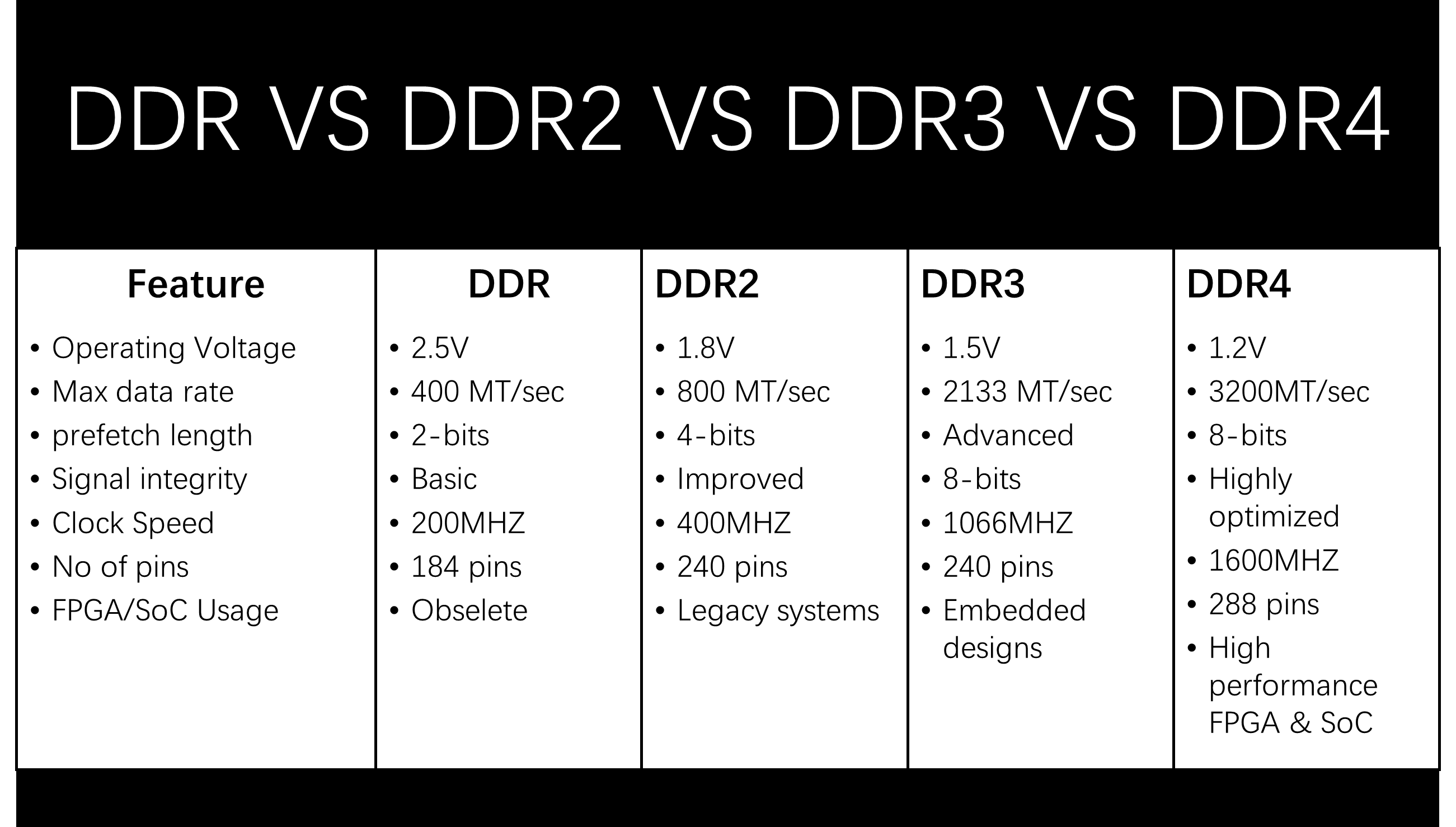
DDR SDRAM (First Generation)
In the year 1998, the first DDR memory was released in the market. First-generation DDR memories use higher voltage (2.5/2.6V), lower speeds (2.1-3.2 GB/s), and consist of only 184 pins. This DDR memory has a prefetch buffer of 2 bits, which is twice that of SDR memory devices.
DDR2 SDRAM (Second Generation)
The second generation of DDR memory has a prefetch buffer of 4 bits, which is double that of the first generation DDR. It has a faster data rate than DDR (4.2-6.4 GB/s) with lower voltage (1.8V) and consists of 240 pins.
DDR3 SDRAM (Third Generation)
The third generation of DDR memory has an increased width of prefetch buffer, which is 8 bits, double of the DDR2 generation. It has higher bandwidth (8.5-14.9 GB/s), lower voltage (1.5V/1.35V), and consists of 240 pins with higher densities.
DDR4 SDRAM (Fourth Generation)
The fourth generation of DDR memory has double the speed of DDR3 and operates on an extremely low voltage of 1.2V. DDR4 has faster (17-21.3+ GB/s), higher chip densities, and consists of 288 pins. It also has some additional features such as CRC and SSN. Some of the most commonly used commonly use industry-proven DDR devices are Micron MT41K256M16 (DDR3), Samsung K4A8G165WB (DDR4), and Micron MT53D512M32 (LPDDR4).
Choosing the Right DDR Module for Your Design
Interfacing DDR memory with the FPGA is the second step. The first and foremost important step before interfacing is identifying the correct DDR memory module for your application. As the incorrect or mismatched DDR for your application can cause issues related to performance, power efficiency, and reliability.
It is therefore, matching a DDR memory is one of the critical task in DDR memory FPGA interfacing. This section will cover a practical guide for selecting the right DDR module for FPGA and SoC designs.
Key Selection Criteria for DDR Memory Modules
While selecting the DDR module, must ensure the following factors before making a decision.
Memory Capacity and Data Width
Depending on your specific application, calculate the total memory size and match the DDR data width, i.e., x8,x16, or x32, with the FPGA/SoC memory controller. For example, Samsung K4A8G165WB (DDR4, x16) is ideal for high-bandwidth applications.
Data Rate and Bandwidth Requirements
It is a fact that higher data rates increase the throughput, but they also demand tight PCB and timing constraints. As we already know, DDR3 supports up to ~2133 MT/s, while DDR4 can exceed 3200 MT/s. It is therefore always select the module whose speed matches your system bandwidth requirements to avoid any mismatch.
Voltage and Power Consumption
As we already know now that DDR4 has the lowest operating voltage (1.2V), and DDR3 has an operating voltage of 1.5V. The lower voltage DDR modules reduce power dissipation and thermal stress. For example, Micron MT53D512M32 (LPDDR4) for battery-powered or thermally constrained systems.
FPGA / SoC Compatibility Considerations
Every DDR module is not always compatible with every FPGA or SoC. Before interfacing make sure that your selected DDR generation supports FPGA/SoC (use datasheet for this purpose). Check supported data widths, maximum speed grades, and voltage rails.
Package Type and Form Factor
Package type and form factor are other important factors that must be considered before choosing the DDR for interfacing with the FPGA. Common packages include FBGA with varying, ball counts and smaller packages reduce board area but also increase routing complexity.

DDR4 Memory Architecture and Pinout
Before we dig into the DDR4 interfacing with FPGA or SoC, it is important first to understand the architecture and its pinout. DDR4 has several improvements over third-generation DDR memory devices, including higher data rates, improved power efficiency, and an extremely low operating voltage of 1.2 volts. However, these advantages come with design complexities, and attention must be given to understand the architecture and pinout of DDR4 memory such that it can be interfaced with an FPGA successfully without any hassle. Samsung K4A8G165WB and Micron MT40A512M16 are some of the most famous examples of DDR4 memory devices.
DDR4 Internal Architecture Overview
At the hardware level, the DDR4 memory is organized into the following architecture.
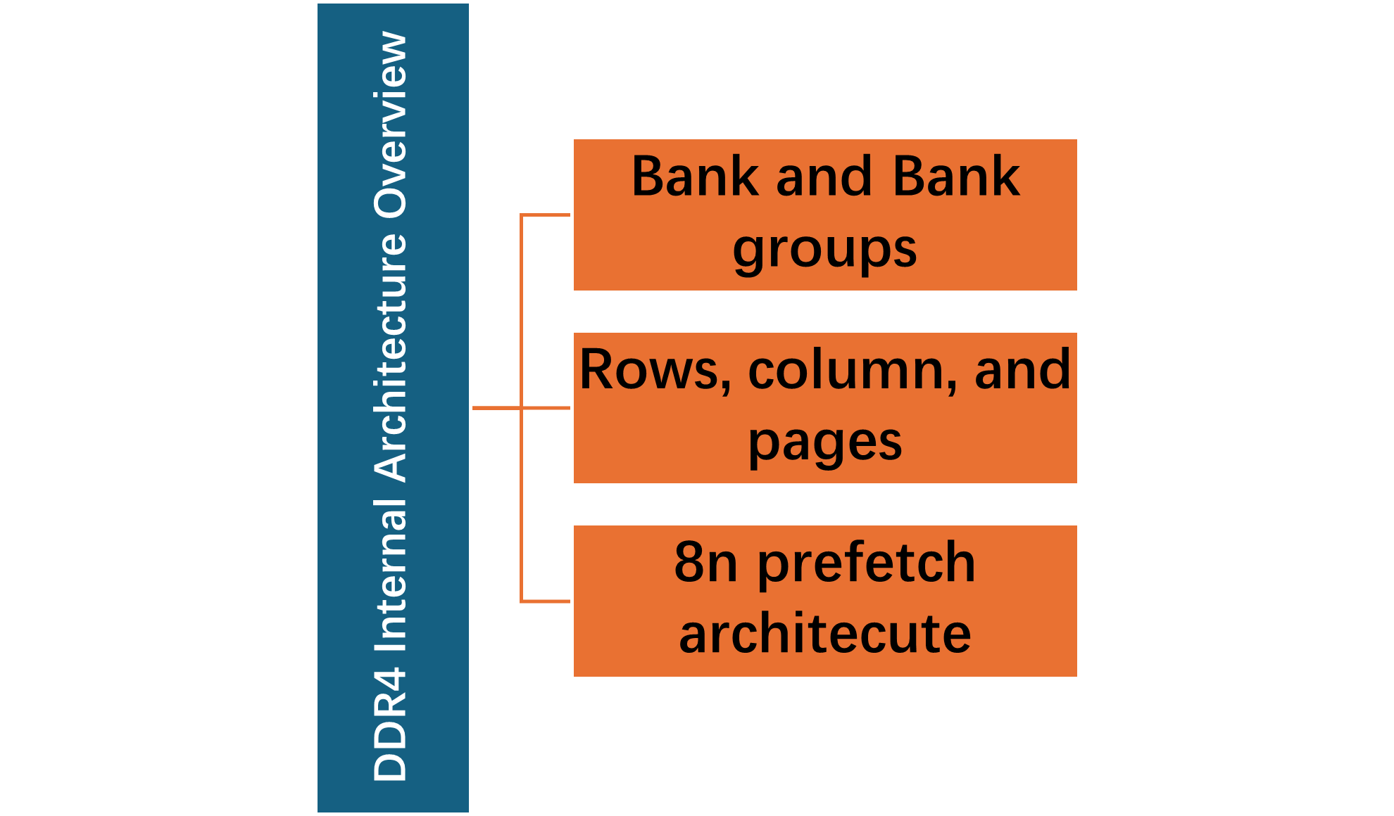
Banks and Bank Groups
The internal architecture of DDR4 memory is divided into multiple banks, which are grouped into banks. These groups are formed to allow higher parallelism and improve bandwidth. This is the major difference between DDR3 and DDR4 memory architecture.
Rows, Columns, and Pages
However, the accessing the memory still follows the row-column architecture same as DDR3. But DDR4 optimized access timing within bank groups.
Prefetch Architecture (8n Prefetch)
As already discussed in the above section that the DDR4 memory devices follow the 8n prefetch architecture. This enables the higher data rates without increasing the core memory clock frequency.
DDR4 Signal Groups and Functional Pin Categories
The DDR4 has 288 pins, and these are logically divided into signal groups which include Data bus, address and command signals, clock signals, control and initialization signals, and power & GND signals.
DDR4 Memory Signal Groups – Functional Overview
Step-by-Step Interfacing Process of DDR4 with FPGA/SoC
At this point, you have built a solid understanding of DDR memory fundamentals and its different types. Now, interfacing DDR4 memory with FPGA requires hardware hardware-aware approach. This section covers a comprehensive step-by-step guide to interfacing DDR4 memory with an FPGA or SoC.
Brief Introduction to DDR4 Types
Technologies are evolving with each passing day, and it is important to keep an eye on newer technologies to make sure you are prepared for the future. There are various DDR4 types available in the market, and you need to make sure that the one you are buying is compatible with your machine. The DDR4 memory devices are categorized further into UDIMM, RDIMM, and SODIMM. By understanding these DDR4 types, you will be able to buy a compatible memory for interfacing with your FPGA.
UDIMM
UDIMM is the Unbuffered Dual In-Line Memory Module, which is widely used DDR4 memory type, especially in consumer electronics, desktop PCs, and workstations. VP9MU2G7228JBHSB – Viking Technology 16 GB DDR4 is the perfect example of UDIMM memory devices.
The key features of UDIMM are;
-data travels directly between the memory controller and DRAM chips.
-No register or buffer between controller and memory
However, these memory devices have limited scalability at high capacities.
The advantages of UDIMM memory devices are that they are cost effective, and consume less power.
RDIMM
RDIMM is Registered Dual In-Line Memory Module and it is designed for servers and enterprise systems. The prime features of RDIMM are;
-Enables higher memory capacities and better signal integrity
-higher latency compared to UDIMM
VP9MR4G7224JBJSB – Viking Technology 32 GB DDR4 is a good example of RDIMM.
SODIMM
SODIMM is the Small Outline Dual In-Line Memory Module, and it is designed for space-constrained systems. Therefore, these are used in laptops, miniPCs, embedded systems, and industrial IoT devices. The prime features of SODIMM are;
-Compact form factor
-Lower maximum capacity than full-size DIMMs
78.C2GF4.4010B – Apacer 8 GB DDR4 SODIMM is one of the example of SODIMM.
DDR4 Memory Type Comparison
Step 1: Understand DDR4 Module Types (UDIMM vs RDIMM vs SODIMM)
Before diving directly into the interfacing, first identify the DDR4 memory type that you want to interface with the FPGA for your application. Once you understand what specific type of DDR4 memory, such as UDIMM, RDIMM, and SODIMM, is suitable/compatible for your application, only then proceed with DDR memory interfacing with the FPGA.
Step 2: Verify FPGA/SoC DDR4 Controller Compatibility
Once the DDR4 memory module is selected, it’s time to carefully select the FPGA with which you want to interface with memory module. Ensure that the selected FPGA supports the selected DDR4 memory module.
To make sure that the DDR memory module and FPGA are compatible, check the following key compatibility checks.
–Support Module Type : UDIMM, RDIMM, or SODIMM support must match the module you selected.
–Bus width and rank support : Check data width (x8, x16, x32) and number of ranks (single vs dual).
–Speed Grade Support: DDR4 modules have max data rates (e.g., 2133 MT/s, 2400 MT/s, 2666 MT/s) and selected FPGA must handle these speeds.
Step 3: Plan Power Rails and Sequencing
DDR4 memory modules require careful power handling must ensure the following power requirements:
- VDD / VDDQ (1.2 V) – Core and I/O power
- VPP (~2.5 V) – Row activation voltage
- VREFCA / VREFDQ – Reference voltages for address/control and data lines
DDR4 memory modules follow a specific power sequence. It is therefore ensure to use the correct power-up sequence: VDD → VDDQ → VPP → VREF. Place decoupling capacitors near DIMM or DRAM pins, and High-capacity modules (32 GB / 64 GB) require higher bulk capacitance.
Step 4: Assign FPGA/SoC Pins and I/O Standards
Correct pin assignment is critical for signal integrity. It is therefore, ensure the following;
- Use dedicated DDR I/O banks
- Match I/O voltage standards to DDR4 module (SSTL or POD)
- Group DQ/DQS signals by byte lane for length matching
Step 5: PCB Layout and Routing
One of the most challenging tasks in DDR memory interfacing with an FPGA is PCB layout. Ensure the following best guidelines for layout and routing:
- Match DQ to DQS trace lengths per byte lane
- Route CK/CK# symmetrically
- Ensure controlled impedance (typically 40–50 Ω differential)
- Minimize vias and stubs
- Place termination and decoupling close to module pins
Step 6: Configure the DDR4 Controller
Use the datasheet of the selected DDR memory module and set the controller parameters. Some of the key controller parameters are module type ((UDIMM/RDIMM/SODIMM) and Speed grade (e.g., 2666 MT/s).
Step 8: Simulate and Verify the DDR4 Interface
Some useful simulation tools such as Vivado and Quartus, allow the user to simulate and verify the DDR4 interface. This will verify the initialization sequence and validate timing closure before hardware.
Step 9: Hardware Bring-Up and Validation
Once everything is all set, you are good to go with powering up the board. After powering up the board, immediately check and verify the power rail and reset signals, and monitor the controller success flags.
Quick Overview: DDR4 Interfacing with FPGA/SoC
For a visual and video tutorial on how to interface DDR4 memory with an FPGA, please follow the video below.
Advanced Applications and Use Cases of DDR4 Memory in FPGA/SoC Designs
In today’s rapidly evolving technological era, DDR4 memory is not a component for basic storage. DDR memory devices enable high performance and bandwidth in modern FPGA and SoC systems. Some of the advanced use cases are discussed in this section to give the engineers or designers an idea about selecting the right DDR memory device for their application.
Machine Learning and AI Acceleration
DDR4 modules are commonly used as working memory for AI accelerators on FPGA or SoC boards. It supports large datasets for real-time inference and batch processing. 32 GB RDIMM (VP9MR4G7224JBJSB) enables multi-channel video analytics or neural network inferencing on embedded platforms.
Video and Image Processing Systems
DDR4 modules are also commonly used with FPGA, enabling HD/4K/8K video processing, encoding, or streaming. SODIMM modules like the Apacer 78.C2GF4.4010B are ideal for compact embedded video devices. The key advantage of these devices is that they minimize frame drops and maintain smooth, low-latency video pipelines.
Conclusion
To sum up, DDR4 memory devices are key components in modern embedded systems because they enable high performance, higher storage capacities, and faster data rates. DDR4 interfacing with FPGA allows the engineers to work on high-performance embedded systems, video processing, and industrial applications. This technical tutorial covers several aspects of DDR4 interfacing with FPGA or SoC, including different types of memory devices, DDR4 types, technological evolution in DDR4 memory devices, and a comprehensive step-by-step guide for engineers and designers on how to interface DDR4 memory with your FPGA for high performance and bandwidth.
Frequently Asked Questions (FAQ)
Ensure your FPGA supports the right DDR4 module type, such as UDIMM, RDIMM, or SODIMM. Check bus width, single/dual rank, speed (2133–2666 MT/s), and ECC support for reliable, high-performance memory integration.
Follow the correct DDR4 power sequence: VDD → VDDQ → VPP → VREF. Use low-noise regulators, proper decoupling near memory pins, and extra bulk capacitance for high-capacity modules (32–64 GB) for stable operation
Use high-capacity UDIMMs (16–64 GB) for AI/ML or networking workloads, SODIMMs for compact embedded systems like robotics or video, and RDIMMs only on server-class FPGA boards with registered DIMM support.
No. RDIMMs require registered DIMM support, which most small FPGAs and SoCs lack. Use UDIMM or SODIMM for embedded and compact designs.
Make sure the DDR4 powers up and resets correctly, confirm the controller has finished training, and run stress tests like read/write loops and burst operations to ensure reliability.