When you start learning about power supplies, one of the first challenges is converting one voltage into another. You may want to change 12 V to 5 V for a microcontroller, boost 5 V up to 12 V for a sensor, or create a small negative voltage for an analog circuit. This is where the MC34063 often becomes the first chip beginners try.
The MC34063 is simple, affordable, and flexible. It can step a voltage down, step it up, or create a negative output using only a few basic components. You do not need advanced tools or complex layouts to make it work.
With the MC34063 datasheet and a handful of parts, you can build a working DC-DC converter even on your first attempt.
In this article, we break the MC34063 down in a very easy way. You will learn what the chip does, how each pin works, and how the internal circuits control the voltage.
We also walk through real examples like a 12 V to 5 V buck converter, a 5 V to 12 V boost circuit, and a simple negative-voltage supply.
By the end, you will know how to confidently use the MC34063 in your own projects without feeling overwhelmed.
MC34063 Overview
The MC34063 is a basic switching-regulator IC that includes an internal transistor, a 1.25 V reference, an oscillator, and current limiting. With just a few external components, it can work as a buck, boost, or inverting converter.
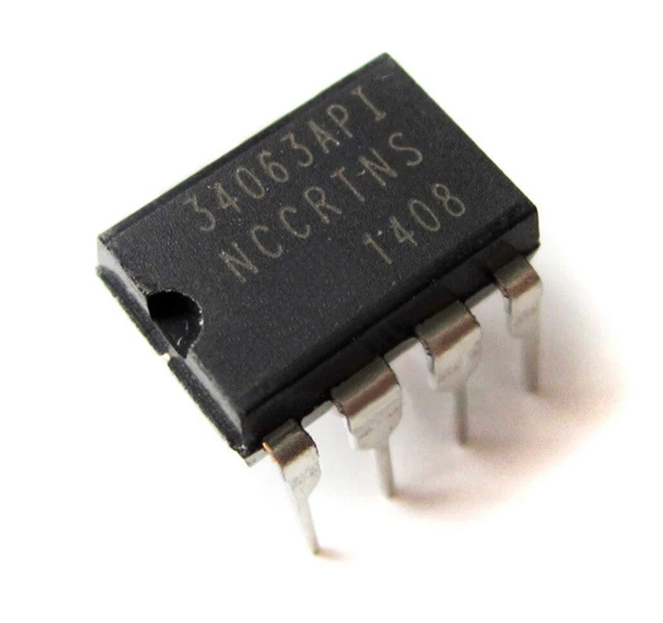
When sourcing the MC34063 itself, you’ll find multiple fully compatible versions from manufacturers like ON Semiconductor, STMicroelectronics, and Texas Instruments.
Popular options such as MC34063ADR (TI), MC34063ACD (Onsemi), and MC34063ACN (ST) are widely available in SOIC-8 and DIP-8 packages.
MC34063 Specifications
Each spec below is taken from ON Semiconductor, STMicroelectronics, and TI versions of the IC, as well as common MC34063 modules sold worldwide.
Overall, these specifications make the MC34063 a flexible, low-risk starting point for almost any small DC-DC project.
How the MC34063 Works
Even though it comes in a tiny 8-pin package, the MC34063 contains almost everything needed to build a full switching power supply.
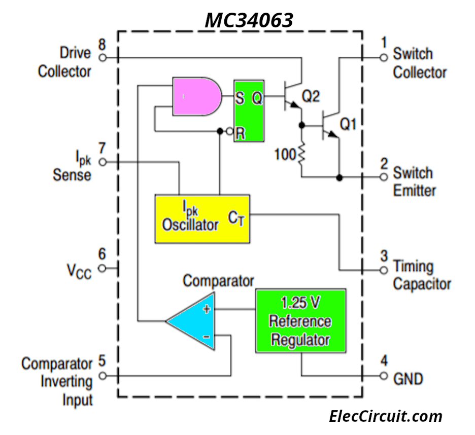
Inside the IC, you’ll find six functional components that shape its behavior:
- 1.25 V Reference
- Comparator for Voltage Regulation
- Oscillator / Timing Generator
- Switching Transistor (Internal Power Switch)
- Current Limiting Circuit
- Driver and Control Logic
These blocks interact to create a complete closed-loop switching system capable of buck, boost, and inverting operation.
The 1.25 V Internal Reference
At the heart of the chip is a precise 1.25 V reference regulator.
All output voltages produced by the MC34063 are compared against this internal reference, which is kept stable across temperature and supply variations.
This is why the output voltage formula is so simple:
\[Vout=1.25×(1+R1R2)\]
That predictability is one of the major reasons engineers still use the MC34063 today.
The Comparator (Feedback Control)
The comparator continuously checks whether the output voltage is:
- Above the target (feedback too high)
- Below the target (feedback too low)
When the output voltage drops slightly, the comparator signals the control logic to increase switching activity.
When the voltage rises, it signals the controller to reduce drive. This forms the regulation loop, ensuring your output stays at the voltage you set with the resistor divider.
Frequency Control
The MC34063 doesn’t come with a fixed switching frequency. Instead, it uses an external timing capacitor on Pin 3 (CT) to set the oscillator frequency.
- A small CT = higher frequency
- A large CT = lower frequency
Most designs run between 20 kHz and 100 kHz, which balances inductor size with efficiency. Datasheets show typical designs around 33–40 kHz for classic applications.
This oscillator defines the Ton/Toff periods, which directly shape the duty cycle.
The Internal Switching Transistor
One of the most important parts of the MC34063 is its internal NPN power switch, capable of 1.5 A peak switch current and up to ~40 V switch voltage
Realistically, you can expect about 0.5–1.0 A continuous output depending on topology and thermal conditions.
The internal transistor replaces the need for an external MOSFET or BJT in lower-power designs, making the MC34063 extremely compact.
- When it turns ON: Current ramps up through the inductor.
- When it turns OFF: The inductor releases energy through the diode into the output.
This is the fundamental switching action behind all converter topologies.
Current Limiting
To prevent overloads, the MC34063 includes a built-in current-limit comparator. You set the limit by connecting a resistor on Pin 7:
\[ I_{limit} \approx \frac{0.3}{R_{SC}} \]
When the switch current reaches approximately 300 mV across RSC, the chip turns the switch off to protect itself and your components.
This is especially important in boost and inverting converters where inductor current can rise quickly.
Control Logic
The control logic acts as the central coordinator inside the MC34063.
It continuously monitors three things: the feedback comparator to see if the output voltage is on target, the oscillator to track timing, and the current-limit circuit to ensure the switch isn’t overloaded.
Using all this information, it decides exactly when to turn the internal transistor on and off, keeping the output voltage stable under changing load and input conditions.
MC34063 Pinout and Pin-by-Pin Explanation
The MC34063 uses an 8-pin layout that keeps the converter design simple while giving you direct control over frequency, current limit, feedback, and switching behavior.
Below is a clear explanation of what each pin does and how it should be connected, based on practical usage and datasheet behavior.

Pin 1 — Vin (Supply Input)
This is the main supply pin. The MC34063 operates from 3 V to 40 V, making it suitable for USB, Li-ion, 12 V rails, and industrial ranges. Add a local bypass capacitor close to this pin to improve stability.
Pin 2 — Switch Collector (SWC)
This connects to the collector of the internal NPN switch. The voltage at this pin swings rapidly during operation, so traces should be short. It connects to Vin in a buck design and to the inductor in a boost design.
Pin 3 — CT (Timing Capacitor)
An external capacitor from CT to ground sets the switching frequency. Smaller values mean higher frequency; larger values produce lower frequency. This capacitor directly affects inductor size, ripple, and efficiency.
Pin 4 — DR (Switch Emitter / Driver Output)
This is the emitter of the internal switch and part of the switching node. It drives the inductor and diode during operation. Because this pin toggles rapidly, minimize wiring length to reduce noise.
Pin 5 — Vfb (Feedback Input)
This pin reads the divided-down output voltage. When Vfb reaches 1.25 V, the chip adjusts the duty cycle to maintain regulation. Keep the feedback path clean and away from switching nodes.
Pin 6 — GND (Ground)
This is the reference ground for the IC. Use a solid ground connection and place sensing and feedback grounds close to this pin to avoid instability.
Pin 7 — Ipk Sense (Current Limit Input)
This pin monitors the voltage across the current-sense resistor RSC. When the voltage reaches about 300 mV, switching stops temporarily to prevent overload. The current limit is set by:
\[ I_{limit} \approx \frac{0.3}{R_{SC}} \]
Pin 8 — VCC (Internal Switch Input / Power Switch Collector)
This powers the internal switching transistor. It handles the main switching current, so keep this trace short and wide. Connection depends on topology: Vin in buck, inductor input in boost, and switching loop in inverting designs.
Feedback traces should avoid switching nodes to prevent oscillation. Switch pins (2 and 4) generate fast edges, so layout quality directly impacts performance.
The CT pin is sensitive to noise; use a stable ceramic capacitor for consistent frequency. The 300 mV current-limit threshold is approximate; use a precise resistor for predictable protection.

Supported Converter Topologies
The MC34063 can operate in three main configurations: buck (step-down), boost (step-up), and inverting (negative output).
These cover almost all small DC-DC conversion needs, which is why “MC34063 buck circuit,” “MC34063 boost circuit,” and “MC34063 inverter” remain highly searched terms.
Buck (Step-Down Conversion)
A buck converter reduces a higher input voltage to a lower, regulated output. With the MC34063, this is one of the easiest configurations to build because the internal switch directly controls the inductor current.
How it works in simple terms:
- When the internal transistor turns ON, current flows from Vin through the inductor and stores energy.
- When the transistor turns OFF, the inductor releases that energy through the Schottky diode into the output capacitor and load.
- The chip adjusts this ON/OFF timing (duty cycle) to hold the output voltage steady.
The output voltage generally follows:
\[ V_{out} \approx V_{in} \cdot D \]
Where D is the duty cycle controlled by the MC34063’s internal feedback loop.
Typical applications
- 12 V → 5 V (logic rails)
- 15 V → 3.3 V (microcontrollers)
- Battery packs → stable low-voltage rails
Usual component choices
- Inductor: 150 µH to 330 µH, rated above 1–1.5 A
- Diode: Schottky, commonly 1N5819
- Output capacitor: Low-ESR electrolytic + 100 nF ceramic
- Switch current: Practical continuous output ~0.7–1 A depending on temperature
Example 1: Simple 12 V to 5 V Buck Converter (500 mA)

This is a very common beginner circuit. It takes 21 V in and produces 5 V at up to 500 mA with much better efficiency than a 7805 linear regulator.
Key parts used:
- L1: 220 µH
- D1: 1N5819 Schottky
- C0: 470 µF output cap
- CT: 470 pF timing capacitor sets the switching frequenc
- R1/R2: Divider to set Vout ≈ 5 V
- RSC: Current-sense resistor (limits peak switch current
Why this circuit works well:
- The MC34063 internal 1.5 A peak transistor is enough for 500 mA output.
- The Schottky diode reduces losses and improves efficiency.
- Only a handful of easy-to-find parts are needed.
- Works well for powering microcontrollers, sensors, GSM modules, and small logic boards.
Example 2: High-Current 2A Buck Converter Using TIP42 PNP Transistor
This is the classic example shown in many MC34063 datasheets and tutorials, and a perfect starting point for beginners.

The MC34063 on its own cannot deliver more than about 0.7–1 A continuously, so for higher loads, an external pass transistor is added. Here, a PNP power transistor TIP42 takes over the heavy current, while the MC34063 only drives the base.
- Input range: 12 V to 30 V
- Output range: Adjustable 2.1 V to 6.9 V
- Current capability: Up to 2 A
How it works:
- The MC34063 still controls switching and regulation
- The TIP42 handles the output current that exceeds the internal transistor limit
- The inductor (220 µH) and diode (1N5822) carry the higher current
- A feedback network with VR1 (10 kΩ pot) allows the user to tune the output voltage.
Why this circuit is useful:
- Allows the MC34063 to power heavier loads like motors, LED arrays, or 5 V SBCs (Raspberry Pi Zero, ESP32 boards)
- External transistor reduces heat stress on the IC
- Still uses inexpensive and commonly available parts
Boost (Step-Up Conversion)
A boost converter takes a low input voltage and raises it to a higher, regulated output. The MC34063 makes this easy because its internal switch controls how the inductor stores and releases energy.
The basic idea is simple:
- When the internal transistor turns ON, the inductor charges and stores energy.
- When the transistor turns OFF, the inductor releases that energy through the diode into the output capacitor.
- Because the inductor “adds” its stored voltage to the input, the output becomes higher than the input.
- The MC34063 controls the duty cycle to maintain the desired output voltage.
The output voltage generally follows:
\[ V_{out} \approx \frac{V_{in}}{1 – D} \]
where D is the duty cycle controlled by the chip.
Typical uses include:
- 5 V → 12 V for sensors or communication modules
- 3.7 V Li-ion → 9–12 V for small amplifiers
- 3.3–5 V → 12 V for radio modules, LED drivers, and test circuits
Important design points:
- Inductor current is significantly higher than the load current, so the inductor must have a high saturation rating.
- A Schottky diode (1N5819, 1N5822) is strongly recommended to reduce losses.
- Output capacitors should have low ESR for stability and clean output.
Example: 3.3V–5V to 12V Boost Converter
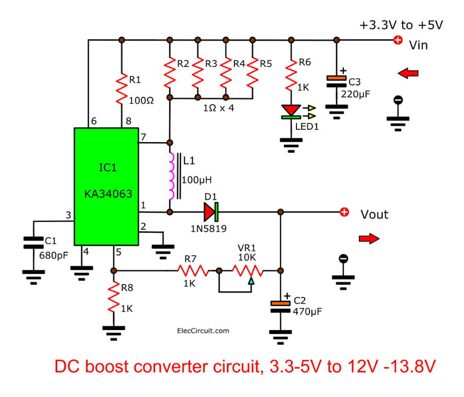
This circuit converts a low-voltage input (3.3–5 V) to around 12–13.8 V at roughly 300–500 mA.
Key components:
- L1: 100 µH inductor (high-current type)
- D1: 1N5819 Schottky diode
- C2/C3: Output and input capacitors for smoothing
- VR1: 10 kΩ adjustable feedback resistor for setting Vout
- R1–R6: Provide current sharing and LED indication
- CT: Timing capacitor (680 pF in the diagram) to set switching frequency
Why this circuit is useful:
- Perfect for boosting small battery sources (Li-ion, AA packs) to 12 V
- Easy to tune using the feedback potentiometer.
- Works well for powering small audio circuits, LED strips, relays, or RF modules.
Example: 12V to 28V Boost Converter
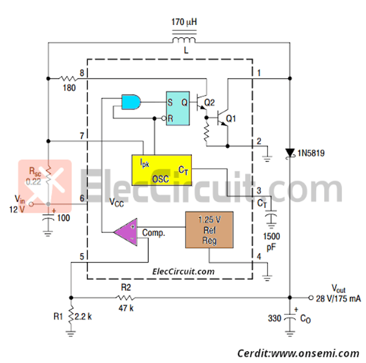
This version shows how the MC34063 can create much higher voltages, such as boosting 12 V up to about 28 V at ~170 mA. It follows the same principle but uses appropriately sized parts.
Key parts:
- L: 170 µH inductor
- CT: ~1500 pF timing capacitor
- D1: 1N5819 diode
- C0: Output capacitor
- R1/R2: Divider to set the higher Vout
Why it works well:
- The internal switch is pushed close to its voltage limit (40 V), but still within safe range.
- Very useful for circuits that require higher rails like Nixie tubes, small motor drivers, or long wiring compensation.
- Only a handful of components are needed, making it cost-effective.
Inverting Converter (Negative Output)
An inverting converter lets you generate a negative voltage from a positive input, which is very useful for op-amp circuits, analog biasing, RS-232 interfaces, sensors, and small audio stages. The MC34063 can do this with only a few components.
The working principle is almost the same as a boost converter, but the energy is routed so that the output sits below ground:
- The inductor charges when the internal switch pulls it to ground.
- When the switch turns OFF, the inductor “flips” its stored energy and sends it through the diode into a capacitor whose negative terminal becomes the output.
- Because this capacitor charges with reversed polarity, the output becomes a stable negative voltage.
The output magnitude still follows the standard MC34063 formula:
\[ \left| V_{out} \right| = 1.25 \left( 1 + \frac{R_2}{R_1} \right) \]
The feedback pin simply monitors the negative output (scaled through R1/R2), and the chip adjusts the duty cycle to keep that voltage constant.
Useful points to keep in mind:
- Inductor and diode selection matters because currents can be higher than the actual load current.
- A Schottky diode such as 1N5819 improves efficiency and reduces losses.
- The output capacitor should be low-ESR since it sits directly in the switching path.
- Layout quality affects ripple; keep the switch loop tight and short.
Example: +5 V to –12 V Converter
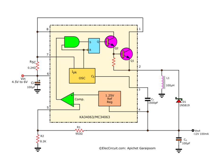
This circuit uses the MC34063 to turn a small positive supply (4.5–6 V) into a clean −12 V output at about 100 mA.
It follows the standard inverting topology but uses carefully chosen parts for stability.
Main components:
- L1: 100 µH inductor
- D1: 1N5819 Schottky (fast recovery, low loss)
- C₀: 100 µF output capacitor rated for negative voltage
- Cᵣ: ~1500 pF timing capacitor to set switching frequency
- R₁/R₂: Divider that programs |Vout| ≈ 12 V
- RSC: 0.24 Ω resistor to set current limit
- CI: 100 µF input capacitor to reduce supply ripple
Why this design works well:
- The MC34063 internal switch handles the required peak current for a ~100 mA negative rail.
- The timing capacitor sets a moderate frequency, keeping inductor size reasonable.
- The Schottky diode improves efficiency and reduces heating.
- The feedback network keeps the −12 V output stable even as load varies.
This topology is commonly used when op-amps or analog stages need a small negative supply without adding a dedicated charge-pump IC.
MC34063 vs Modern DC-DC Converters
The MC34063 is a flexible and inexpensive switch-mode controller, but it comes from an older generation of power ICs.
Modern regulators like the LM2596, XL4015, and TPS5430 deliver higher current, better efficiency, and improved thermal handling.
Understanding these differences helps you choose the right IC based on load, efficiency needs, and topology (buck, boost, or inverting).
MC34063 vs LM2596
The LM2596 is one of the most popular buck regulators used in ready-made step-down modules. It can supply up to 3 A with efficiencies around 90% or higher.
Its internal MOSFET and fixed 150 kHz switching frequency give it stable ripple performance and make the design much simpler—no timing capacitor or external current-sense resistor is required.
The MC34063, however, supports three topologies (buck, boost, and inverting), making it more flexible in small projects. It is inexpensive, works well below about 0.7–1 A, and is extremely easy to build on perfboard or breadboard.
Use LM2596 when:
- you need higher current
- efficiency matters
- you want low ripple with minimal tuning
Use MC34063 when you want a cheap, simple, multi-topology converter.
MC34063 vs XL4015
The XL4015 is designed for high-current buck applications. It supplies up to 5 A, often with efficiency above 92%, and includes built-in thermal and overcurrent protection.
It is popular in adjustable power supplies, battery charging circuits, and LED drivers. The MC34063 is still more suitable for:
- compact, low-power designs
- boost and inverting circuits (which XL4015 cannot provide)
- very low-cost builds with a small BOM
The XL4015 wins easily for high-power buck converters, but the MC34063 remains a smart choice for light loads and non-buck topologies.
MC34063 vs TPS5430
The TPS5430 is a more modern and refined buck controller from Texas Instruments. It delivers 3 A continuously and switches at 570 kHz, allowing the use of much smaller inductors and capacitors.
It also handles transients very well and includes modern protection features like cycle-by-cycle current limiting and thermal shutdown.
The MC34063 still has an advantage when the design requires:
- a boost converter
- a negative voltage rail
- a simple, low-cost power stage under 1 A
TPS5430 is ideal for compact, efficient buck converters; MC34063 is ideal when you need flexibility or non-buck configurations.
When the MC34063 Is Still a Good Choice
Even though it’s old, the MC34063 still fits many real-world needs. It performs well in the 0.1–0.7 A range, works reliably in boost and inverting designs, and is perfect for low-cost or educational projects.
It also remains useful for maintaining older hardware where the original converter must be preserved.
Final Thoughts
The MC34063 may not be a modern regulator, but it still holds a strong place in low and medium-power electronics. Its wide input range, simple 1.25 V reference, and built-in switch make it surprisingly capable for small designs.
With just a few external parts, it can handle buck, boost, and inverting converters, which is why it continues to appear in hobby projects, educational kits, and even older commercial hardware.
Of course, this flexibility comes with limits. Its efficiency normally stays between 60% and 85%, and the internal switch peaks at about 1.5 A.
For learners, hobbyists, and small-volume builders, the MC34063 remains a reliable workhorse. It is forgiving, easy to experiment with, and inexpensive enough that mistakes are part of the learning process rather than a setback.
If you are ready to build your own supply, Flywing Tech offers the full set of parts you need. You can source MC34063 ICs, inductors, Schottky diodes, capacitors, connectors, and wiring accessories.
MC34063 FAQ
1. What is the MC34063 used for?
The MC34063 is a DC-DC converter IC that can create step-down (buck), step-up (boost), and negative (inverting) voltages using only a few external components. It’s widely used in small power supplies and hobby electronics.
2. Is the MC34063 still used today?
Yes. Even though it’s an older design, the MC34063 remains popular in low-cost devices, automotive accessories, repair work, and educational circuits because it is cheap, flexible, and easy to understand.
3. What voltage range can the MC34063 accept?
It works from 3 V to 40 V, making it suitable for USB power, Li-ion batteries, 12 V systems, and even industrial 24 V rails.
4. How much current can the MC34063 deliver?
Its internal switch can handle 1.5 A peak, but real-world continuous output is usually 0.5–1.0 A depending on cooling and the conversion mode. Higher current is possible with an external transistor.
5. What types of converters can I build with the MC34063?
You can build:
- Buck converters (step-down)
- Boost converters (step-up)
- Inverting converters (negative voltage)
This versatility is one of the main reasons the chip is still widely used.
6. Why do MC34063 circuits use Schottky diodes?
Schottky diodes have:
- Fast switching
- Low forward voltage
- Lower heat loss
They significantly improve efficiency and stability in MC34063 designs.
7. Is the MC34063 suitable for beginners?
Absolutely. It’s one of the easiest switching-regulator ICs to learn because:
- It uses simple external components
- Datasheet formulas are straightforward
- DIP-8 versions work on breadboards
- You can build buck, boost, and inverting designs with the same chip
8. When should I not use the MC34063?
Avoid using it when you need:
- Very high efficiency
- More than 1–1.5 A output
- Low ripple for sensitive digital circuits
- Very small inductors or high-frequency switching
Modern ICs like LM2596, XL4015, or TPS5430 perform better in these cases.
9. Can the MC34063 boost 5 V up to 12 V?
Yes. It can reliably convert 5 V to 12 V for loads around 200–500 mA, depending on the inductor and diode used. It’s a common use case for sensors, amplifiers, and communication modules.
All the components required to build buck, boost, and inverting MC34063 supplies are available in one place.