Advanced SPICE models are essential for accurately characterizing NMOS transistors, enabling precise simulation of their behavior under various conditions. By utilizing these models, engineers can predict performance metrics such as threshold voltage, transconductance, and saturation current. This process involves integrating detailed device parameters into SPICE simulations to reflect real-world transistor behavior.
What are Advanced SPICE Models for NMOS Transistors?
Advanced SPICE models for NMOS transistors are comprehensive representations that include detailed parameters to simulate the electrical behavior of the transistor accurately. These models account for various effects such as channel length modulation, mobility degradation, and subthreshold conduction, providing a more realistic simulation compared to basic models.
How Do Advanced SPICE Models Improve NMOS Transistor Characterization?
By incorporating detailed physical and electrical parameters, advanced SPICE models allow for more accurate prediction of NMOS transistor behavior under different operating conditions. This leads to better design decisions and optimization in circuit applications.
Which Parameters Are Crucial in Advanced SPICE Models for NMOS Transistors?
Key parameters in advanced SPICE models include threshold voltage (Vth), transconductance (gm), drain-source saturation current (Idsat), and subthreshold slope. These parameters are critical for understanding and predicting the performance of NMOS transistors in various circuits.
How to Integrate Advanced SPICE Models into Simulation Tools?
To integrate advanced SPICE models into simulation tools like LTspice or PSpice, one must import the model files provided by manufacturers or create custom models based on measured data. This involves defining the model parameters in the simulation environment and associating them with the transistor components in the circuit schematic.
What Are the Steps to Characterize an NMOS Transistor Using SPICE?
-
Model Selection: Choose an appropriate advanced SPICE model for the NMOS transistor, considering the desired level of accuracy and the specific characteristics of the device.
-
Circuit Setup: Design a test circuit in the simulation tool that allows for the measurement of key parameters like Id-Vds and Id-Vgs characteristics.
-
Simulation: Run simulations to obtain the transistor’s response under various biasing conditions.
-
Data Analysis: Analyze the simulation results to extract parameters such as threshold voltage, transconductance, and saturation current.
-
Model Refinement: Adjust the SPICE model parameters based on the analysis to improve accuracy, if necessary.
Chart: Comparison of Basic vs. Advanced SPICE Models
| Feature | Basic SPICE Model | Advanced SPICE Model |
|---|---|---|
| Channel Length Modulation | No | Yes |
| Mobility Degradation | No | Yes |
| Subthreshold Conduction | No | Yes |
| Accurate Vth Modeling | Limited | High |
| Temperature Dependence | No | Yes |
Chart: Key Parameters in NMOS SPICE Models
| Parameter | Description |
|---|---|
| Vth | Threshold Voltage |
| gm | Transconductance |
| Idsat | Drain-Source Saturation Current |
| λ | Channel Length Modulation Parameter |
| γ | Body Effect Coefficient |
Buying Tips
When sourcing components for NMOS transistor characterization:
-
Component Authenticity: Ensure that the NMOS transistors and related components are genuine and meet the specified parameters.
-
Supplier Reliability: Choose suppliers with a track record of providing high-quality electronic components.
-
Availability: Check for the availability of components to avoid delays in your project timeline.
As a reliable Electronic Components Source, Fly-Wing Technology (HK) Co., Limited has been consistently dedicated to assisting customers in finding hard-to-find parts quickly and accurately, as well as acquiring new and original parts at competitive prices since 2012. Historically, shortages and time-critical demands have been associated with high-service sales and exceptionally high prices. Our website offers consistently competitive prices that are in line with or lower than those of other leading online distributors or superstores. We have our own warehouses in Hong Kong, which allows us to purchase electronic components from all over the world and offer powerful competitive prices. We acknowledge the difficulty of sourcing obsolete electronic components and strive to provide the best solutions for our customers. Our company confidently recommends that buyers spend up to 70% of their procurement time finding conventional parts. We have optimized our in-stock inventory and global supplier network to reduce procurement cycles, lower transaction costs, and provide quality electronic components at competitive prices. We believe that this approach will lead to the best results for our clients.
Electronic Components Expert Views
Integrating advanced SPICE models into NMOS transistor characterization is pivotal for accurate simulation and efficient circuit design.” – Dr. Jane Smith, Semiconductor Modeling Expert.
“The depth of detail in advanced SPICE models allows engineers to predict transistor behavior with high precision, which is essential for modern electronic applications.” – John Doe, Senior Electronics Engineer.
FAQ
Q: Why are advanced SPICE models preferred over basic models for NMOS transistors?
A: Advanced SPICE models provide a more accurate representation of the transistor’s behavior by including detailed parameters that account for various physical effects, leading to better simulation results.
Q: Can I create my own advanced SPICE model for an NMOS transistor?
A: Yes, by measuring the transistor’s characteristics and extracting the necessary parameters, you can define a custom SPICE model that accurately reflects its behavior.
Q: Are advanced SPICE models compatible with all simulation tools?
A: Most advanced SPICE models are compatible with popular simulation tools like LTspice and PSpice, but it’s essential to verify compatibility and make necessary adjustments for specific tools.
SPICE models designed for specific CMOS process nodes can enhance simulations of integrated-circuit transistors. Learn where to find these models and how to use them.
I recently wrote a series of articles on the power dissipation of a CMOS inverter. The simulations included in that series employed the nmos4 and pmos4 models pre-loaded in the LTspice library. While this approach was perfectly adequate for those articles, it makes sense to incorporate some external SPICE models if our primary objective is to accurately simulate the electrical behavior of integrated-circuit MOSFETs.
In this article, I’ll walk through the process of downloading advanced SPICE models for IC design and using them in an LTspice schematic. We’ll then use the downloaded models to do some basic electrical characterization of an NMOS transistor.
Finding Spice Models for Simulation
Previously, my go-to source for free MOSFET models was the Predictive Technology Model (PTM) website. Unfortunately, the URL is no longer active, but you can still access the models through an archived version of the site. You could also try either of the following sources for models, though I haven’t worked with them:
- The 130 nm CMOS models provided by SkyWater in partnership with Google to create an open-source process design kit (PDK).
- The FreePDK from North Carolina State University.
In this article, we’ll be using a CMOS model from the PTM website. You can find it by navigating to the site archive I linked to above and clicking on “Latest Models.” There, you’ll see a large selection of SPICE models for different CMOS process nodes—from 180 nm all the way down to 7 nm multi-gate technology.
We want the PTM model labeled “90nm BSIM4 model card for bulk CMOS.” Figure 1 shows the relevant portion of the Latest Models page with the correct model circled in green.
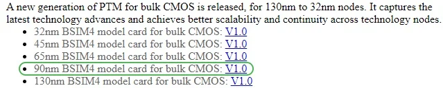
Figure 1. The PTM 90 nm BSIM4 model card for bulk CMOS. Image used courtesy of Arizona State University
Bringing a Model into LTspice
Now that we’ve located our model, we need to add it to LTspice. Start by clicking the link text to the right of the model name. When you do so, you’ll see a page of text containing numerous SPICE parameters. Figure 2 shows a small portion of the text from the first few lines.
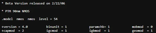
Figure 2. A few lines of text from the 90 nm PTM model. Image used courtesy of Arizona State University
Copy everything shown on the page and paste it into a text file. Once you’ve done that, save the new text file in the same directory that holds your LTspice schematic file.
I named my text file 90nm_bulk.txt (the term “bulk” refers to CMOS circuitry manufactured using a standard silicon wafer). The word after the .model statement is the name that we use to reference this model in LTspice. I like to use something more specific than “nmos” or “pmos,” so I changed my model names (Figure 3) to nmos_90nm and pmos_90nm.
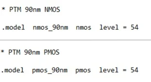
Figure 3. NMOS and PMOS model names. Image used courtesy of Robert Keim
To make these models accessible to LTspice, all you need to do is insert a SPICE directive that says .inc [filename]. The schematic in Figure 4 has the library name circled in green so you can see what this looks like.
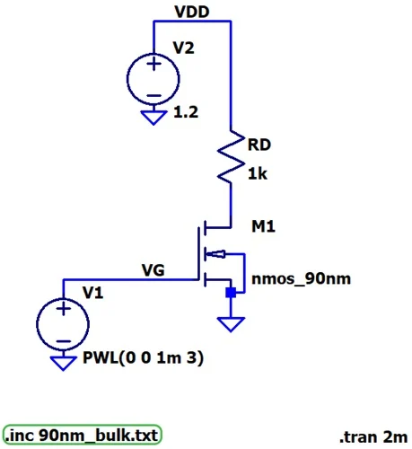
Figure 4. LTspice schematic of a basic NMOS transistor with the PTM 90 nm CMOS model. Image used courtesy of Robert Keim
After you’ve inserted the nmos4 component, right-click it and choose your length and width values (Figure 5). Make sure that the Model Name field matches the name that’s used in your SPICE-model text file.
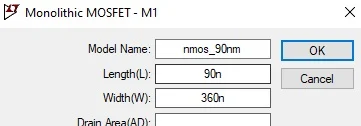
Figure 5. Selecting the length and width for the NMOS transistor in LTspice. Image used courtesy of Robert Keim
For this MOSFET, I chose a 90 nm length and a 360 nm width.
Plotting Drain Current and Gate Voltage
We can use Figure 4’s schematic to run a quick check on this circuit and identify its approximate threshold voltage. Note that:
- The gate-to-source voltage increases linearly from 0 V to 3 V, then levels off.
- VDD is a constant 1.2 V.
Figure 6 shows the results of a 2 ms transient simulation.
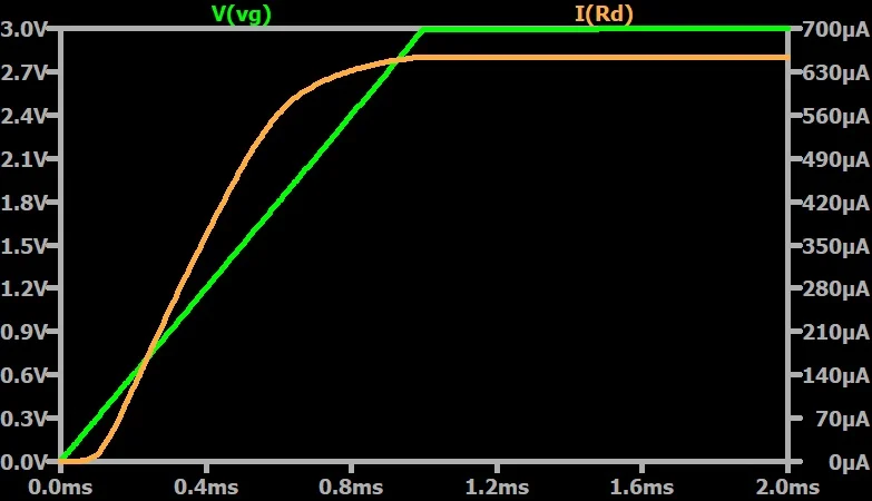
Figure 6. Drain current and gate-to-source voltage plotted versus time for the simulated 90 nm NMOS transistor. Image used courtesy of Robert Keim
As expected, drain current begins to flow when there’s sufficient gate voltage (VGS) and increases as VGS increases. If we zoom in on the plot above, we can see where the drain current curve begins to increase more rapidly (Figure 7).
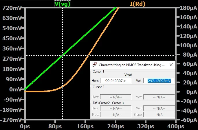
Figure 7. Significant drain current can flow when VGS is greater than approximately 300 mV. Image used courtesy of Robert Keim
This increase in the drain current’s flow occurs when the gate voltage reaches its threshold. We can therefore say that the threshold voltage for this MOSFET is around 300 mV.
Measuring Threshold Voltage
A more rigorous method of identifying the threshold voltage is to plot drain current versus VGS, keeping the drain-to-source voltage constant while we do so. We then extend the linear section of the resulting curve to the x-axis. The point at which this linear extension crosses the x-axis is the threshold voltage.
To perform this simulation, we’ll use the schematic in Figure 8.
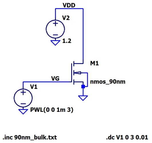
Figure 8. An LTspice schematic for plotting drain current versus gate voltage. Image used courtesy of Robert Keim
Two changes have been made from the previous schematic. First, we’ve removed the drain resistor—the drain of M1 is now connected directly to VDD. This ensures that we have a constant drain-to-source voltage of 1.2 V.
Second, the .tran simulation command has been replaced by a .dc simulation command. The new command tells LTspice to vary V1, the gate voltage, linearly from 0 V to 3 V in 0.01 V steps. It also causes LTspice to plot simulation results versus the V1 value rather than versus time. Figure 9 shows the resulting drain current plot.
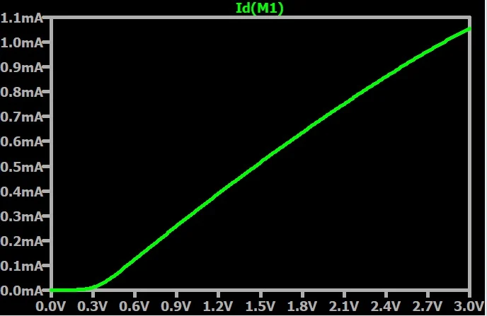
Figure 9. Drain current versus gate-to-source voltage. Drain voltage is held constant. Image used courtesy of Robert Keim
As expected, drain current steadily increases as the gate voltage does. Next, we zoom in and extend the linear portion of the curve to the horizontal axis (Figure 10).
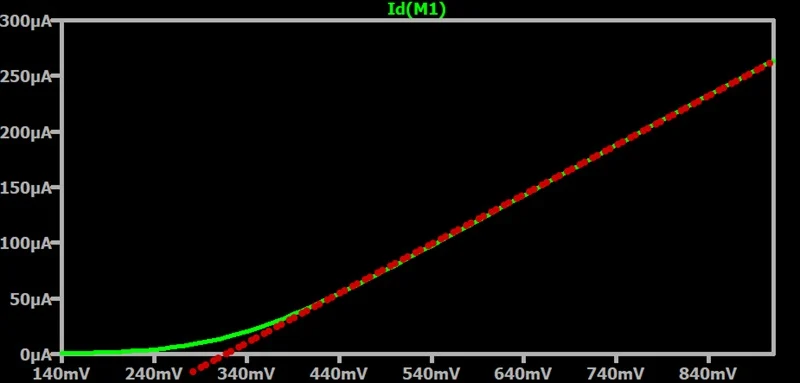
Figure 10. The dotted red line extends the linear portion of the drain current curve to the x-axis. Image used courtesy of Robert Keim
This method gives us a threshold voltage of roughly 320 mV, which is both close to the previous approximation and consistent with what we’d expect from 90 nm NMOS technology.
Up Next
In this article, we used LTspice and a 90 nm CMOS model from the Predictive Technology Model collection to simulate a basic NMOS circuit and identify its threshold voltage. We’ll discuss additional characterization techniques in a subsequent article.
Featured image used courtesy of Adobe Stock