STF34NM60ND
RoHS  RoHS compliant
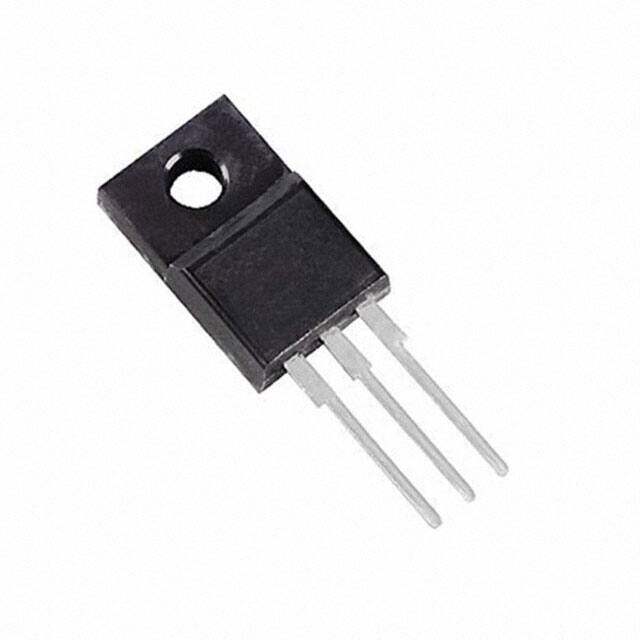
Package TO-220-3 Full Pack
Category Discrete Semiconductor Products / Transistors - FETs, MOSFETs - Single
Description
MOSFET N-Ch 600V 0.097 Ohm 29A FDmesh II
PDF
/
Buying Options
Total Price: USD $16.11
Unit Price: USD $16.10915
≥1 USD $16.10915
≥10 USD $13.2183
≥100 USD $12.80505
≥500 USD $12.3918
≥1000 USD $11.97855
Inventory: 7609
Minimum: 1
-
+

Technical Details
Compliance
Lead Free Lead Free
RoHS Status ROHS3 Compliant
REACH SVHC No SVHC
Radiation Hardening No
Dimensions
Width 4.6mm
Length 10.4mm
Height 16.4mm
Technical
Pulsed Drain Current-Max (IDM) 116A
Drain to Source Breakdown Voltage 650V
Gate to Source Voltage (Vgs) 25V
JEDEC-95 Code TO-220AB
Threshold Voltage 4V
Continuous Drain Current (ID) 29A
Turn-Off Delay Time 111 ns
Fall Time (Typ) 61.8 ns
Vgs (Max) ±25V
Drive Voltage (Max Rds On,Min Rds On) 10V
Drain to Source Voltage (Vdss) 600V
Rise Time 53.4 ns
Gate Charge (Qg) (Max) @ Vgs 80.4nC @ 10V
Current - Continuous Drain (Id) @ 25°C 29A Tc
Input Capacitance (Ciss) (Max) @ Vds 2785pF @ 50V
Vgs(th) (Max) @ Id 5V @ 250μA
Rds On (Max) @ Id, Vgs 110m Ω @ 14.5A, 10V
Transistor Application SWITCHING
FET Type N-Channel
Turn On Delay Time 30 ns
Case Connection ISOLATED
Power Dissipation 190W
Operating Mode ENHANCEMENT MODE
Element Configuration Single
Power Dissipation-Max 40W Tc
Number of Elements 1
Pin Count 3
Base Part Number STF34N
Technology MOSFET (Metal Oxide)
Subcategory FET General Purpose Power
Additional Feature ULTRA-LOW RESISTANCE
Terminal Finish Matte Tin (Sn) - annealed
Resistance 105MOhm
ECCN Code EAR99
Number of Terminations 3
Moisture Sensitivity Level (MSL) 1 (Unlimited)
Part Status Active
JESD-609 Code e3
Series FDmesh? II
Packaging Tube
Operating Temperature 150°C TJ
Physical
Transistor Element Material SILICON
Number of Pins 3
Package / Case TO-220-3 Full Pack
Mounting Type Through Hole
Mount Through Hole
Supply Chain
Factory Lead Time 16 Weeks
Alternative Model

Recommended For You

STF34NM60ND+price,STF34NM60ND+datasheet,STF34NM60ND+in stock,buy+STF34NM60ND,finder+STF34NM60ND,STF34NM60ND+tutorials,STF34NM60ND+download