FDB024N06
RoHS  RoHS compliant
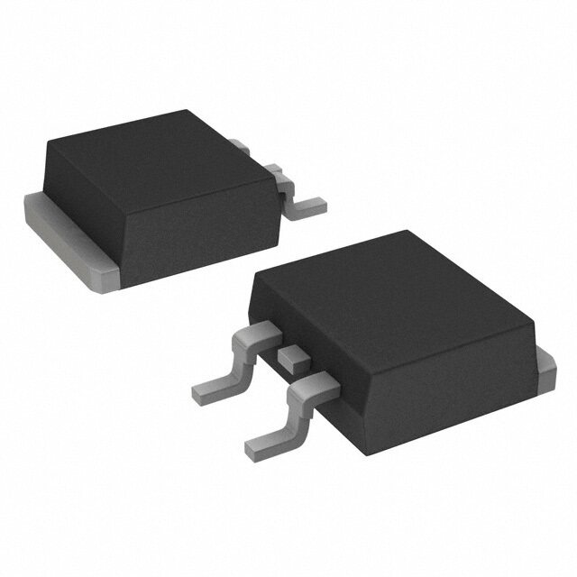
Package TO-263-3, D2Pak (2 Leads + Tab), TO-263AB
Category Discrete Semiconductor Products / Transistors - FETs, MOSFETs - Single
Description
MOSFET N-CH 60V 120A D2PAK
PDF
/
Buying Options
Total Price: USD $4.55
Unit Price: USD $4.5496
≥1 USD $4.5496
≥10 USD $3.81744
≥100 USD $3.088184
Inventory: 1185
Minimum: 1
-
+

Technical Details
Compliance
Lead Free Lead Free
RoHS Status ROHS3 Compliant
REACH SVHC No SVHC
Radiation Hardening No
Dimensions
Width 9.65mm
Length 10.67mm
Height 4.83mm
Technical
Drain to Source Breakdown Voltage 60V
Gate to Source Voltage (Vgs) 20V
Threshold Voltage 3.5V
Continuous Drain Current (ID) 265A
Turn-Off Delay Time 348 ns
Fall Time (Typ) 250 ns
Vgs (Max) ±20V
Drive Voltage (Max Rds On,Min Rds On) 10V
Rise Time 324 ns
Gate Charge (Qg) (Max) @ Vgs 226nC @ 10V
Current - Continuous Drain (Id) @ 25°C 120A Tc
Input Capacitance (Ciss) (Max) @ Vds 14885pF @ 25V
Vgs(th) (Max) @ Id 4.5V @ 250μA
Rds On (Max) @ Id, Vgs 2.4m Ω @ 75A, 10V
Transistor Application SWITCHING
FET Type N-Channel
Turn On Delay Time 134 ns
Case Connection DRAIN
Power Dissipation 395W
Operating Mode ENHANCEMENT MODE
Element Configuration Single
Power Dissipation-Max 395W Tc
Number of Elements 1
JESD-30 Code R-PSSO-G2
Terminal Form GULL WING
Technology MOSFET (Metal Oxide)
Subcategory FET General Purpose Power
Terminal Finish Tin (Sn)
Resistance 2.4MOhm
ECCN Code EAR99
Number of Terminations 2
Moisture Sensitivity Level (MSL) 1 (Unlimited)
Part Status Active
Pbfree Code yes
JESD-609 Code e3
Series PowerTrench?
Published 2013
Packaging Tape & Reel (TR)
Operating Temperature -55°C~175°C TJ
Physical
Transistor Element Material SILICON
Weight 1.762g
Number of Pins 3
Package / Case TO-263-3, D2Pak (2 Leads + Tab), TO-263AB
Mounting Type Surface Mount
Mount Surface Mount
Supply Chain
Lifecycle Status ACTIVE (Last Updated: 4 days ago)
Factory Lead Time 8 Weeks
Alternative Model

Recommended For You

FDB024N06+price,FDB024N06+datasheet,FDB024N06+in stock,buy+FDB024N06,finder+FDB024N06,FDB024N06+tutorials,FDB024N06+download