TT8M3TR
RoHS  RoHS compliant
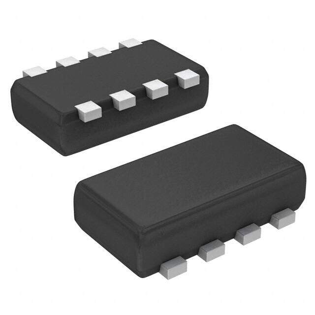
Package 8-SMD, Flat Lead
Category Discrete Semiconductor Products / Transistors - FETs, MOSFETs - Arrays
Description
MOSFET N/P-CH 20V 2.5A TSST8
PDF
/
Buying Options
Total Price: USD $0.81
Unit Price: USD $0.8056
≥1 USD $0.8056
≥10 USD $0.6612
≥100 USD $0.6403
≥500 USD $0.62035
≥1000 USD $0.59945
Inventory: 1130
Minimum: 1
-
+

Technical Details
Compliance
RoHS Status ROHS3 Compliant
Lead Free Lead Free
Technical
FET Feature Logic Level Gate, 1.5V Drive
FET Technology METAL-OXIDE SEMICONDUCTOR
DS Breakdown Voltage-Min 20V
Drain-source On Resistance-Max 0.09Ohm
Drain Current-Max (Abs) (ID) 2.5A
Continuous Drain Current (ID) 2.4A
Polarity/Channel Type N-CHANNEL AND P-CHANNEL
Drain to Source Voltage (Vdss) 20V
Gate Charge (Qg) (Max) @ Vgs 3.6nC @ 4.5V
Current - Continuous Drain (Id) @ 25°C 2.5A 2.4A
Input Capacitance (Ciss) (Max) @ Vds 260pF @ 10V
Vgs(th) (Max) @ Id 1V @ 1mA
Rds On (Max) @ Id, Vgs 72m Ω @ 2.5A, 4.5V
Transistor Application SWITCHING
FET Type N and P-Channel
Operating Mode ENHANCEMENT MODE
Configuration SEPARATE, 2 ELEMENTS WITH BUILT-IN DIODE
Number of Elements 2
Qualification Status Not Qualified
JESD-30 Code R-PDSO-F8
Pin Count 8
Time@Peak Reflow Temperature-Max (s) 10
Peak Reflow Temperature (Cel) 260
Terminal Position DUAL
Max Power Dissipation 1W
Subcategory Other Transistors
Terminal Finish TIN COPPER
ECCN Code EAR99
Number of Terminations 8
Moisture Sensitivity Level (MSL) 1 (Unlimited)
Part Status Not For New Designs
Pbfree Code yes
JESD-609 Code e2
Published 2010
Packaging Cut Tape (CT)
Operating Temperature 150°C TJ
Physical
Transistor Element Material SILICON
Package / Case 8-SMD, Flat Lead
Mounting Type Surface Mount
Mount Surface Mount
Supply Chain
Factory Lead Time 10 Weeks
Alternative Model

Recommended For You

TT8M3TR+price,TT8M3TR+datasheet,TT8M3TR+in stock,buy+TT8M3TR,finder+TT8M3TR,TT8M3TR+tutorials,TT8M3TR+download