SI8489EDB-T2-E1
RoHS  RoHS compliant
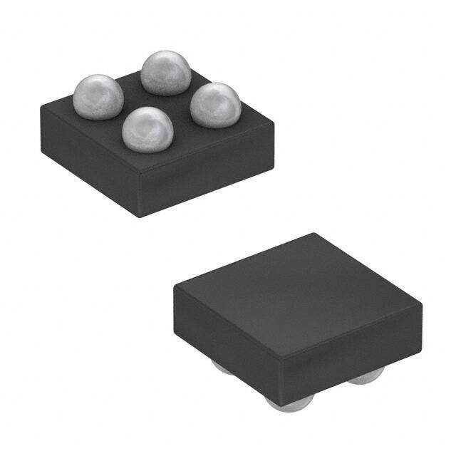
Package 4-UFBGA
Category Discrete Semiconductor Products / Transistors - FETs, MOSFETs - Single
Description
SI8489EDB-T2-E1 P-channel MOSFET Transistor; 4.3 A; 20 V; 4-Pin MICRO FOOT
PDF
/
Buying Options
Total Price: USD $0.4
Unit Price: USD $0.396
≥1 USD $0.396
≥10 USD $0.34144
≥100 USD $0.237072
≥500 USD $0.185117
≥1000 USD $0.150462
Inventory: 1108
Minimum: 1
-
+

Technical Details
Compliance
RoHS Status ROHS3 Compliant
Radiation Hardening No
Technical
Drain to Source Breakdown Voltage -20V
Gate to Source Voltage (Vgs) 12V
Continuous Drain Current (ID) 5.4A
Turn-Off Delay Time 50 ns
Fall Time (Typ) 25 ns
Vgs (Max) ±12V
Drive Voltage (Max Rds On,Min Rds On) 2.5V 10V
Drain to Source Voltage (Vdss) 20V
Rise Time 20ns
Gate Charge (Qg) (Max) @ Vgs 27nC @ 10V
Input Capacitance (Ciss) (Max) @ Vds 765pF @ 10V
Vgs(th) (Max) @ Id 1.2V @ 250μA
Rds On (Max) @ Id, Vgs 44m Ω @ 1.5A, 10V
Transistor Application SWITCHING
FET Type P-Channel
Turn On Delay Time 27 ns
Power Dissipation 1.8W
Operating Mode ENHANCEMENT MODE
Element Configuration Single
Power Dissipation-Max 780mW Ta 1.8W Tc
Number of Channels 1
Number of Elements 1
Terminal Form BALL
Terminal Position BOTTOM
Technology MOSFET (Metal Oxide)
ECCN Code EAR99
Number of Terminations 4
Moisture Sensitivity Level (MSL) 1 (Unlimited)
Part Status Active
Series TrenchFET?
Published 2015
Packaging Tape & Reel (TR)
Operating Temperature -55°C~150°C TJ
Physical
Transistor Element Material SILICON
Number of Pins 4
Package / Case 4-UFBGA
Mounting Type Surface Mount
Mount Surface Mount
Contact Plating Tin
Supply Chain
Factory Lead Time 33 Weeks
Alternative Model

Recommended For You

SI8489EDB-T2-E1+price,SI8489EDB-T2-E1+datasheet,SI8489EDB-T2-E1+in stock,buy+SI8489EDB-T2-E1,finder+SI8489EDB-T2-E1,SI8489EDB-T2-E1+tutorials,SI8489EDB-T2-E1+download