SI8461DB-T2-E1
RoHS  RoHS compliant
Package 4-XFBGA, CSPBGA
Category Discrete Semiconductor Products / Transistors - FETs, MOSFETs - Single
Description
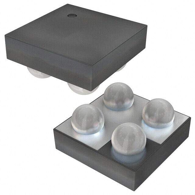
SI8461DB-T2-E1 P-channel MOSFET Transistor; 3 A; 20 V; 4-Pin MICRO FOOT
PDF
/
Buying Options
Total Price: USD $0.33
Unit Price: USD $0.3325
≥1 USD $0.3325
≥10 USD $0.27265
≥100 USD $0.2641
≥500 USD $0.25555
≥1000 USD $0.247
Inventory: 1175
Minimum: 1
-
+

Technical Details
Compliance
Lead Free Lead Free
RoHS Status ROHS3 Compliant
REACH SVHC Unknown
Radiation Hardening No
Technical
Drain to Source Breakdown Voltage -20V
Drain Current-Max (Abs) (ID) 2.5A
Gate to Source Voltage (Vgs) 8V
Threshold Voltage -1V
Continuous Drain Current (ID) -3.7A
Turn-Off Delay Time 35 ns
Fall Time (Typ) 10 ns
Vgs (Max) ±8V
Drive Voltage (Max Rds On,Min Rds On) 1.5V 4.5V
Drain to Source Voltage (Vdss) 20V
Rise Time 25 ns
Gate Charge (Qg) (Max) @ Vgs 24nC @ 8V
Input Capacitance (Ciss) (Max) @ Vds 610pF @ 10V
Vgs(th) (Max) @ Id 1V @ 250μA
Rds On (Max) @ Id, Vgs 100m Ω @ 1.5A, 4.5V
Transistor Application SWITCHING
FET Type P-Channel
Turn On Delay Time 15 ns
Power Dissipation 780mW
Operating Mode ENHANCEMENT MODE
Element Configuration Single
Power Dissipation-Max 780mW Ta 1.8W Tc
Number of Channels 1
Number of Elements 1
Pin Count 4
Time@Peak Reflow Temperature-Max (s) 30
Peak Reflow Temperature (Cel) 260
Terminal Form BALL
Terminal Position BOTTOM
Technology MOSFET (Metal Oxide)
Subcategory Other Transistors
Terminal Finish Matte Tin (Sn)
Resistance 100mOhm
ECCN Code EAR99
Number of Terminations 4
Moisture Sensitivity Level (MSL) 1 (Unlimited)
Part Status Obsolete
Pbfree Code yes
JESD-609 Code e3
Series TrenchFET?
Published 2013
Packaging Tape & Reel (TR)
Operating Temperature -55°C~150°C TJ
Physical
Transistor Element Material SILICON
Number of Pins 4
Package / Case 4-XFBGA, CSPBGA
Mounting Type Surface Mount
Mount Surface Mount
Supply Chain
Factory Lead Time 15 Weeks
Alternative Model

Recommended For You

SI8461DB-T2-E1+price,SI8461DB-T2-E1+datasheet,SI8461DB-T2-E1+in stock,buy+SI8461DB-T2-E1,finder+SI8461DB-T2-E1,SI8461DB-T2-E1+tutorials,SI8461DB-T2-E1+download