SI8402DB-T1-E1
RoHS  RoHS compliant
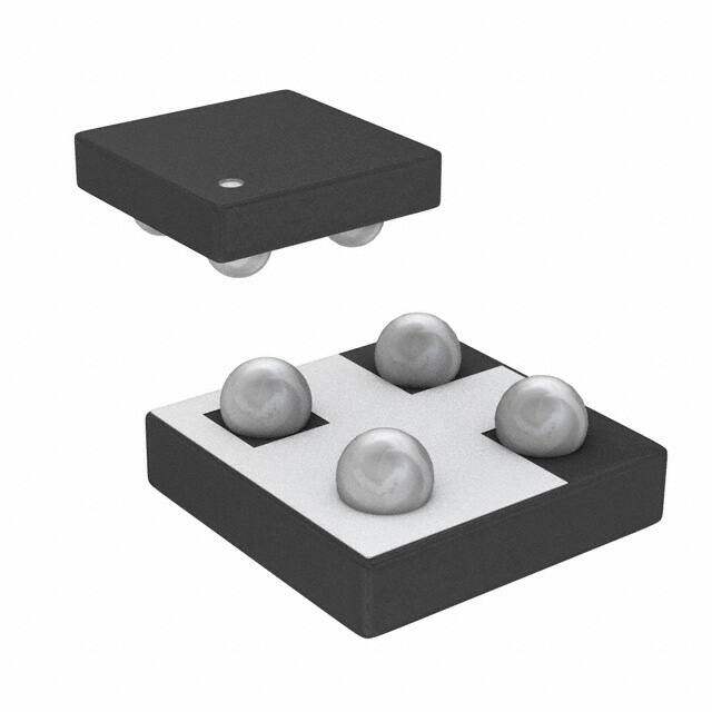
Package 4-XFBGA, CSPBGA
Category Discrete Semiconductor Products / Transistors - FETs, MOSFETs - Single
Description
MOSFET N-CH 20V 5.3A 2X2 4-MFP
PDF
/
Buying Options
Total Price: USD $0.55
Unit Price: USD $0.5529
≥1 USD $0.5529
≥10 USD $0.4541
≥100 USD $0.43985
≥500 USD $0.4256
≥1000 USD $0.41135
Inventory: 1138
Minimum: 1
-
+

Technical Details
Compliance
Lead Free Lead Free
RoHS Status ROHS3 Compliant
Radiation Hardening No
Dimensions
Width 1.6002mm
Length 1.5748mm
Height 355.6μm
Technical
Drain to Source Breakdown Voltage 20V
Drain Current-Max (Abs) (ID) 5.3A
Gate to Source Voltage (Vgs) 8V
Continuous Drain Current (ID) 7.3A
Turn-Off Delay Time 45 ns
Fall Time (Typ) 145 ns
Rise Time 145 ns
Gate Charge (Qg) (Max) @ Vgs 26nC @ 4.5V
Current - Continuous Drain (Id) @ 25°C 5.3A Ta
Vgs(th) (Max) @ Id 1V @ 250μA
Rds On (Max) @ Id, Vgs 37m Ω @ 1A, 4.5V
Transistor Application SWITCHING
FET Type N-Channel
Turn On Delay Time 30 ns
Power Dissipation 1.47W
Operating Mode ENHANCEMENT MODE
Element Configuration Single
Number of Elements 1
Pin Count 4
Time@Peak Reflow Temperature-Max (s) 40
Peak Reflow Temperature (Cel) 260
Terminal Form BALL
Terminal Position BOTTOM
Technology MOSFET (Metal Oxide)
Max Power Dissipation 1.47W
Subcategory FET General Purpose Power
Min Operating Temperature -55°C
Max Operating Temperature 150°C
Terminal Finish Matte Tin (Sn)
Resistance 37MOhm
ECCN Code EAR99
Number of Terminations 4
Moisture Sensitivity Level (MSL) 1 (Unlimited)
Part Status Obsolete
Pbfree Code yes
JESD-609 Code e3
Series TrenchFET?
Published 2016
Packaging Cut Tape (CT)
Physical
Number of Pins 4
Package / Case 4-XFBGA, CSPBGA
Mounting Type Surface Mount
Mount Surface Mount
Alternative Model

Recommended For You
SI8402DB-T1-E1+price,SI8402DB-T1-E1+datasheet,SI8402DB-T1-E1+in stock,buy+SI8402DB-T1-E1,finder+SI8402DB-T1-E1,SI8402DB-T1-E1+tutorials,SI8402DB-T1-E1+download