SI7806ADN-T1-E3
RoHS  RoHS compliant
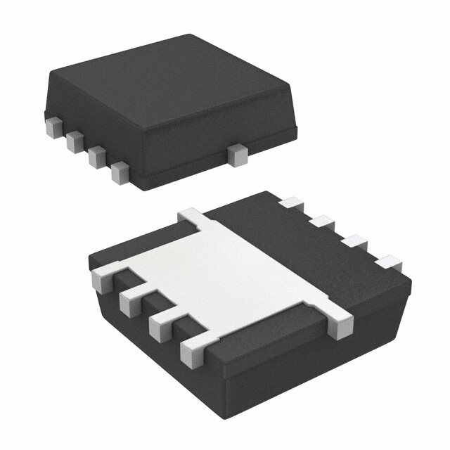
Package PowerPAK? 1212-8
Category Discrete Semiconductor Products / Transistors - FETs, MOSFETs - Single
Description
MOSFET N-CH 30V 9A 1212-8
PDF
/
Buying Options
Total Price: USD $1.23
Unit Price: USD $1.232
≥1 USD $1.232
≥10 USD $1.0076
≥100 USD $0.783904
≥500 USD $0.66447
≥1000 USD $0.541279
Inventory: 117
Minimum: 1
-
+

Technical Details
Compliance
RoHS Status ROHS3 Compliant
Radiation Hardening No
Dimensions
Width 3.05mm
Length 3.05mm
Height 1.04mm
Technical
DS Breakdown Voltage-Min 30V
Pulsed Drain Current-Max (IDM) 40A
Drain Current-Max (Abs) (ID) 9A
Gate to Source Voltage (Vgs) 20V
Continuous Drain Current (ID) 9A
Turn-Off Delay Time 33 ns
Fall Time (Typ) 10 ns
Vgs (Max) ±20V
Drive Voltage (Max Rds On,Min Rds On) 4.5V 10V
Drain to Source Voltage (Vdss) 30V
Rise Time 10 ns
Gate Charge (Qg) (Max) @ Vgs 20nC @ 5V
Current - Continuous Drain (Id) @ 25°C 9A Ta
Vgs(th) (Max) @ Id 3V @ 250μA
Rds On (Max) @ Id, Vgs 11m Ω @ 14A, 10V
Transistor Application SWITCHING
FET Type N-Channel
Turn On Delay Time 13 ns
Case Connection DRAIN
Power Dissipation 1.5W
Operating Mode ENHANCEMENT MODE
Element Configuration Single
Power Dissipation-Max 1.5W Ta
Number of Channels 1
Number of Elements 1
JESD-30 Code S-XDSO-C5
Pin Count 8
Time@Peak Reflow Temperature-Max (s) 30
Peak Reflow Temperature (Cel) 260
Terminal Form C BEND
Terminal Position DUAL
Technology MOSFET (Metal Oxide)
Subcategory FET General Purpose Power
ECCN Code EAR99
Number of Terminations 5
Moisture Sensitivity Level (MSL) 1 (Unlimited)
Part Status Active
Pbfree Code yes
JESD-609 Code e3
Series TrenchFET?
Published 2017
Packaging Tape & Reel (TR)
Operating Temperature -55°C~150°C TJ
Physical
Transistor Element Material SILICON
Number of Pins 8
Package / Case PowerPAK? 1212-8
Mounting Type Surface Mount
Mount Surface Mount
Contact Plating Tin
Supply Chain
Factory Lead Time 14 Weeks
Alternative Model

Recommended For You

SI7806ADN-T1-E3+price,SI7806ADN-T1-E3+datasheet,SI7806ADN-T1-E3+in stock,buy+SI7806ADN-T1-E3,finder+SI7806ADN-T1-E3,SI7806ADN-T1-E3+tutorials,SI7806ADN-T1-E3+download