SI3454ADV-T1-E3
RoHS  RoHS compliant
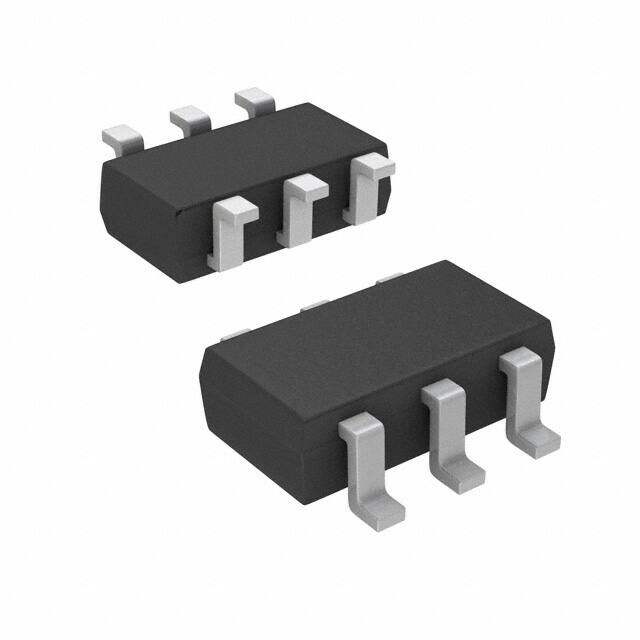
Package SOT-23-6 Thin, TSOT-23-6
Category Discrete Semiconductor Products / Transistors - FETs, MOSFETs - Single
Description
MOSFET N-CH 30V 3.4A 6-TSOP
PDF
/
Buying Options
Total Price: USD $0.83
Unit Price: USD $0.8303
≥1 USD $0.8303
≥10 USD $0.68115
≥100 USD $0.66025
≥500 USD $0.6384
≥1000 USD $0.6175
Inventory: 2367
Minimum: 1
-
+

Technical Details
Technical
Rise Time 10 ns
Drive Voltage (Max Rds On,Min Rds On) 4.5V 10V
Vgs (Max) ±20V
Fall Time (Typ) 10 ns
Turn-Off Delay Time 20 ns
Continuous Drain Current (ID) 3.4A
Threshold Voltage 3V
Gate to Source Voltage (Vgs) 20V
Drain to Source Breakdown Voltage 30V
Dual Supply Voltage 30V
Nominal Vgs 3 V
Gate Charge (Qg) (Max) @ Vgs 15nC @ 10V
Current - Continuous Drain (Id) @ 25°C 3.4A Ta
Vgs(th) (Max) @ Id 3V @ 250μA
Rds On (Max) @ Id, Vgs 60m Ω @ 4.5A, 10V
FET Type N-Channel
Turn On Delay Time 10 ns
Power Dissipation 1.14W
Operating Mode ENHANCEMENT MODE
Current 34A
Element Configuration Single
Power Dissipation-Max 1.14W Ta
Voltage 30V
Number of Elements 1
Pin Count 6
Time@Peak Reflow Temperature-Max (s) 40
Peak Reflow Temperature (Cel) 260
Terminal Form GULL WING
Terminal Position DUAL
Technology MOSFET (Metal Oxide)
Subcategory FET General Purpose Power
Terminal Finish Matte Tin (Sn)
Resistance 60mOhm
ECCN Code EAR99
Termination SMD/SMT
Number of Terminations 6
Moisture Sensitivity Level (MSL) 1 (Unlimited)
Part Status Obsolete
Pbfree Code yes
JESD-609 Code e3
Series TrenchFET?
Published 2016
Packaging Tape & Reel (TR)
Operating Temperature -55°C~150°C TJ
Dimensions
Height 1mm
Length 3.05mm
Width 1.65mm
Compliance
Radiation Hardening No
REACH SVHC No SVHC
RoHS Status ROHS3 Compliant
Lead Free Lead Free
Physical
Transistor Element Material SILICON
Number of Pins 6
Package / Case SOT-23-6 Thin, TSOT-23-6
Mounting Type Surface Mount
Mount Surface Mount
Alternative Model

Recommended For You

SI3454ADV-T1-E3+price,SI3454ADV-T1-E3+datasheet,SI3454ADV-T1-E3+in stock,buy+SI3454ADV-T1-E3,finder+SI3454ADV-T1-E3,SI3454ADV-T1-E3+tutorials,SI3454ADV-T1-E3+download