IRFU9014PBF
RoHS  RoHS compliant
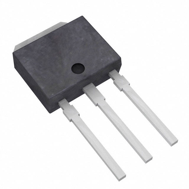
Package TO-251-3 Short Leads, IPak, TO-251AA
Category Discrete Semiconductor Products / Transistors - FETs, MOSFETs - Single
Description
MOSFET P-CH 60V 5.1A I-PAK
PDF
/
Buying Options
Total Price: USD $1.29
Unit Price: USD $1.2936
≥1 USD $1.2936
≥10 USD $1.036288
≥100 USD $0.821278
≥500 USD $0.696106
≥1000 USD $0.567054
≥3000 USD $0.533817
Inventory: 499
Minimum: 1
-
+

Technical Details
Compliance
Lead Free Lead Free
RoHS Status ROHS3 Compliant
REACH SVHC Unknown
Radiation Hardening No
Dimensions
Width 2.39mm
Length 6.73mm
Height 6.22mm
Technical
Nominal Vgs -4 V
Pulsed Drain Current-Max (IDM) 20A
Drain to Source Breakdown Voltage -60V
Gate to Source Voltage (Vgs) 20V
Threshold Voltage -4V
Continuous Drain Current (ID) 5.1A
Turn-Off Delay Time 9.6 ns
Fall Time (Typ) 31 ns
Vgs (Max) ±20V
Drive Voltage (Max Rds On,Min Rds On) 10V
Drain to Source Voltage (Vdss) 60V
Rise Time 63 ns
Gate Charge (Qg) (Max) @ Vgs 12nC @ 10V
Current - Continuous Drain (Id) @ 25°C 5.1A Tc
Input Capacitance (Ciss) (Max) @ Vds 270pF @ 25V
Vgs(th) (Max) @ Id 4V @ 250μA
Rds On (Max) @ Id, Vgs 500m Ω @ 3.1A, 10V
Transistor Application SWITCHING
FET Type P-Channel
Turn On Delay Time 11 ns
Case Connection DRAIN
Power Dissipation 2.5W
Operating Mode ENHANCEMENT MODE
Element Configuration Single
Power Dissipation-Max 2.5W Ta 25W Tc
Number of Channels 1
Number of Elements 1
Lead Length 9.65mm
Pin Count 3
Time@Peak Reflow Temperature-Max (s) 40
Peak Reflow Temperature (Cel) 260
Technology MOSFET (Metal Oxide)
Subcategory Other Transistors
Additional Feature AVALANCHE RATED
Terminal Finish Matte Tin (Sn)
Resistance 500mOhm
ECCN Code EAR99
Number of Terminations 3
Moisture Sensitivity Level (MSL) 1 (Unlimited)
Part Status Active
Pbfree Code yes
JESD-609 Code e3
Published 2008
Packaging Tube
Operating Temperature -55°C~150°C TJ
Physical
Transistor Element Material SILICON
Weight 329.988449mg
Number of Pins 3
Package / Case TO-251-3 Short Leads, IPak, TO-251AA
Mounting Type Through Hole
Mount Through Hole
Supply Chain
Factory Lead Time 8 Weeks
Alternative Model

Recommended For You

IRFU9014PBF+price,IRFU9014PBF+datasheet,IRFU9014PBF+in stock,buy+IRFU9014PBF,finder+IRFU9014PBF,IRFU9014PBF+tutorials,IRFU9014PBF+download