CSD25483F4
RoHS  RoHS compliant
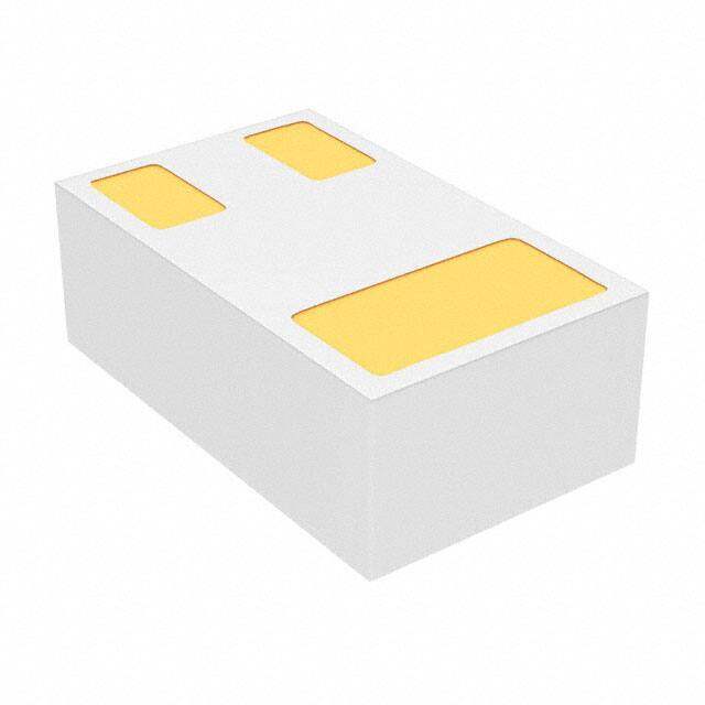
Package 3-XFDFN
Category Discrete Semiconductor Products / Transistors - FETs, MOSFETs - Single
Description
MOSFET P-CH 20V LGA
PDF
/
Buying Options
Total Price: USD $0.36
Unit Price: USD $0.3608
≥1 USD $0.3608
≥10 USD $0.25432
≥100 USD $0.128304
≥500 USD $0.104702
≥1000 USD $0.077678
Inventory: 1182
Minimum: 1
-
+

Technical Details
Compliance
Lead Free Lead Free
RoHS Status ROHS3 Compliant
Dimensions
Width 635μm
Length 1.035mm
Technical
Drain to Source Breakdown Voltage -20V
Gate to Source Voltage (Vgs) -12V
Continuous Drain Current (ID) 1.6A
Turn-Off Delay Time 17.4 ns
Fall Time (Typ) 7 ns
Drive Voltage (Max Rds On,Min Rds On) 1.8V 4.5V
Drain to Source Voltage (Vdss) 20V
Rise Time 3.7ns
Gate Charge (Qg) (Max) @ Vgs 0.959nC @ 4.5V
Current - Continuous Drain (Id) @ 25°C 1.6A Ta
Input Capacitance (Ciss) (Max) @ Vds 198pF @ 10V
Vgs(th) (Max) @ Id 1.2V @ 250μA
Rds On (Max) @ Id, Vgs 205m Ω @ 500mA, 8V
FET Type P-Channel
Turn On Delay Time 4.3 ns
Operating Mode -0.95
Element Configuration Single
Power Dissipation-Max 500mW Ta
Number of Channels 1
Base Part Number CSD25483
Time@Peak Reflow Temperature-Max (s) NOT SPECIFIED
Peak Reflow Temperature (Cel) 260
Terminal Form NO LEAD
Terminal Position BOTTOM
Technology MOSFET (Metal Oxide)
ECCN Code EAR99
Moisture Sensitivity Level (MSL) 1 (Unlimited)
Part Status Active
Pbfree Code yes
Series NexFET?
Packaging Tape & Reel (TR)
Operating Temperature -55°C~150°C TJ
Physical
Number of Pins 3
Package / Case 3-XFDFN
Mounting Type Surface Mount
Mount Surface Mount
Supply Chain
Lifecycle Status ACTIVE (Last Updated: 3 days ago)
Factory Lead Time 6 Weeks
Alternative Model

Recommended For You
CSD25483F4+price,CSD25483F4+datasheet,CSD25483F4+in stock,buy+CSD25483F4,finder+CSD25483F4,CSD25483F4+tutorials,CSD25483F4+download