CSD25481F4T
RoHS  RoHS compliant
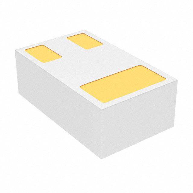
Package 3-XFDFN
Category Discrete Semiconductor Products / Transistors - FETs, MOSFETs - Single
Description
TEXAS INSTRUMENTS CSD25481F4T MOSFET Transistor, P Channel, -2.5 A, -20 V, 0.075 ohm, -8 V, -950 mV
PDF
/
Buying Options
Total Price: USD $0.53
Unit Price: USD $0.528
≥1 USD $0.528
≥10 USD $0.43384
≥100 USD $0.337216
Inventory: 1231
Minimum: 1
-
+

Technical Details
Compliance
Lead Free Lead Free
RoHS Status ROHS3 Compliant
REACH SVHC No SVHC
Dimensions
Width 635μm
Length 1.035mm
Height 350μm
Technical
Drain to Source Breakdown Voltage -20V
Gate to Source Voltage (Vgs) 12V
Threshold Voltage -950mV
Continuous Drain Current (ID) 2.5A
Turn-Off Delay Time 16.9 ns
Fall Time (Typ) 6.7 ns
Vgs (Max) -12V
Drive Voltage (Max Rds On,Min Rds On) 1.8V 4.5V
Drain to Source Voltage (Vdss) 20V
Rise Time 3.6 ns
Gate Charge (Qg) (Max) @ Vgs 0.91nC @ 4.5V
Current - Continuous Drain (Id) @ 25°C 2.5A Ta
Input Capacitance (Ciss) (Max) @ Vds 189pF @ 10V
Vgs(th) (Max) @ Id 1.2V @ 250μA
Rds On (Max) @ Id, Vgs 88m Ω @ 500mA, 8V
Transistor Application SWITCHING
FET Type P-Channel
Turn On Delay Time 4.1 ns
Power Dissipation 500mW
Operating Mode ENHANCEMENT MODE
Element Configuration Single
Power Dissipation-Max 500mW Ta
Number of Channels 1
Number of Elements 1
Base Part Number CSD25481
Time@Peak Reflow Temperature-Max (s) NOT SPECIFIED
Peak Reflow Temperature (Cel) 260
Terminal Form NO LEAD
Terminal Position BOTTOM
Technology MOSFET (Metal Oxide)
Additional Feature ULTRA LOW RESISTANCE
ECCN Code EAR99
Number of Terminations 3
Moisture Sensitivity Level (MSL) 1 (Unlimited)
Part Status Active
Pbfree Code yes
Series FemtoFET?
Packaging Tape & Reel (TR)
Operating Temperature -55°C~150°C TJ
Physical
Transistor Element Material SILICON
Number of Pins 3
Package / Case 3-XFDFN
Mounting Type Surface Mount
Mount Surface Mount
Supply Chain
Lifecycle Status ACTIVE (Last Updated: 3 days ago)
Factory Lead Time 6 Weeks
Alternative Model

Recommended For You

CSD25481F4T+price,CSD25481F4T+datasheet,CSD25481F4T+in stock,buy+CSD25481F4T,finder+CSD25481F4T,CSD25481F4T+tutorials,CSD25481F4T+download