CSD25404Q3
RoHS  RoHS compliant
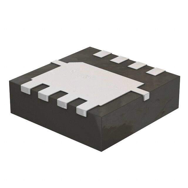
Package 8-PowerVDFN
Category Discrete Semiconductor Products / Transistors - FETs, MOSFETs - Single
Description
MOSFET P-CH 20V 104A 8VSON
PDF
/
Buying Options
Total Price: USD $0.87
Unit Price: USD $0.86732
≥1 USD $0.86732
≥10 USD $0.81823
≥100 USD $0.77191
≥500 USD $0.72822
≥1000 USD $0.687
Inventory: 2875
Minimum: 1
-
+

Technical Details
Compliance
Lead Free Contains Lead
RoHS Status ROHS3 Compliant
Dimensions
Thickness 1mm
Width 3.3mm
Length 3.3mm
Technical
DS Breakdown Voltage-Min 20V
Pulsed Drain Current-Max (IDM) 240A
Drain-source On Resistance-Max 0.0121Ohm
Gate to Source Voltage (Vgs) 12V
Continuous Drain Current (ID) 104A
Turn-Off Delay Time 35 ns
Fall Time (Typ) 13 ns
Vgs (Max) ±12V
Drive Voltage (Max Rds On,Min Rds On) 1.8V 4.5V
Drain to Source Voltage (Vdss) 20V
Rise Time 8ns
Gate Charge (Qg) (Max) @ Vgs 14.1nC @ 4.5V
Current - Continuous Drain (Id) @ 25°C 104A Tc
Input Capacitance (Ciss) (Max) @ Vds 2120pF @ 10V
Vgs(th) (Max) @ Id 1.15V @ 250μA
Rds On (Max) @ Id, Vgs 6.5m Ω @ 10A, 4.5V
Transistor Application SWITCHING
FET Type P-Channel
Turn On Delay Time 13 ns
Case Connection SOURCE
Operating Mode ENHANCEMENT MODE
Element Configuration Single
Power Dissipation-Max 2.8W Ta 96W Tc
Number of Elements 1
Base Part Number CSD25404
Reach Compliance Code not_compliant
Terminal Form NO LEAD
Terminal Position DUAL
Technology MOSFET (Metal Oxide)
ECCN Code EAR99
Number of Terminations 5
Moisture Sensitivity Level (MSL) 1 (Unlimited)
Part Status Active
Pbfree Code yes
JESD-609 Code e3
Series NexFET?
Packaging Tape & Reel (TR)
Operating Temperature -55°C~150°C TJ
Physical
Transistor Element Material SILICON
Number of Pins 8
Package / Case 8-PowerVDFN
Mounting Type Surface Mount
Mount Surface Mount
Contact Plating Tin
Supply Chain
Lifecycle Status ACTIVE (Last Updated: 4 days ago)
Factory Lead Time 12 Weeks
Alternative Model

Recommended For You

CSD25404Q3+price,CSD25404Q3+datasheet,CSD25404Q3+in stock,buy+CSD25404Q3,finder+CSD25404Q3,CSD25404Q3+tutorials,CSD25404Q3+download