CSD19503KCS
RoHS  RoHS compliant
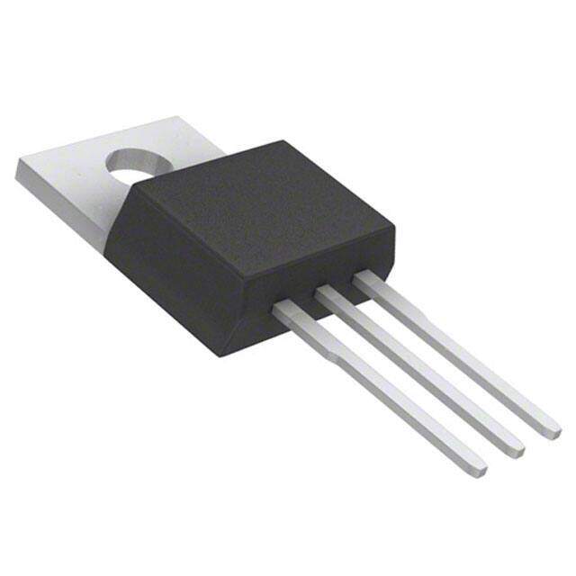
Package TO-220-3
Category Discrete Semiconductor Products / Transistors - FETs, MOSFETs - Single
Description
MOSFET N-CH 80V 94A TO220-3
PDF
/
Buying Options
Total Price: USD $1.47
Unit Price: USD $1.4696
≥1 USD $1.4696
≥10 USD $1.179552
≥100 USD $0.970552
≥500 USD $0.821251
≥1000 USD $0.696819
≥3000 USD $0.66198
Inventory: 415
Minimum: 1
-
+

Technical Details
Compliance
Lead Free Lead Free
RoHS Status ROHS3 Compliant
REACH SVHC No SVHC
Dimensions
Thickness 4.58mm
Width 8.7mm
Length 10.16mm
Height 4.7mm
Technical
DS Breakdown Voltage-Min 80V
Pulsed Drain Current-Max (IDM) 247A
Drain Current-Max (Abs) (ID) 94A
Gate to Source Voltage (Vgs) 20V
Threshold Voltage 2.8V
Continuous Drain Current (ID) 100A
Turn-Off Delay Time 11 ns
Fall Time (Typ) 2 ns
Vgs (Max) ±20V
Drive Voltage (Max Rds On,Min Rds On) 6V 10V
Drain to Source Voltage (Vdss) 80V
Rise Time 3 ns
Gate Charge (Qg) (Max) @ Vgs 36nC @ 10V
Current - Continuous Drain (Id) @ 25°C 100A Ta
Input Capacitance (Ciss) (Max) @ Vds 2730pF @ 40V
Vgs(th) (Max) @ Id 3.4V @ 250μA
Rds On (Max) @ Id, Vgs 9.2m Ω @ 60A, 10V
Transistor Application SWITCHING
FET Type N-Channel
Turn On Delay Time 7 ns
Case Connection DRAIN
Power Dissipation 188W
Operating Mode ENHANCEMENT MODE
Element Configuration Single
Power Dissipation-Max 188W Tc
Number of Channels 1
Number of Elements 1
Base Part Number CSD19503
Time@Peak Reflow Temperature-Max (s) NOT SPECIFIED
Reach Compliance Code not_compliant
Peak Reflow Temperature (Cel) NOT SPECIFIED
Technology MOSFET (Metal Oxide)
Subcategory FET General Purpose Power
Additional Feature AVALANCHE RATED
ECCN Code EAR99
Number of Terminations 3
Moisture Sensitivity Level (MSL) 1 (Unlimited)
Part Status Active
Pbfree Code yes
JESD-609 Code e3
Series NexFET?
Packaging Tube
Operating Temperature -55°C~175°C TJ
Physical
Transistor Element Material SILICON
Weight 6.000006g
Number of Pins 3
Package / Case TO-220-3
Mounting Type Through Hole
Mount Through Hole
Contact Plating Tin
Supply Chain
Lifecycle Status ACTIVE (Last Updated: 6 days ago)
Factory Lead Time 6 Weeks
Alternative Model

Recommended For You

CSD19503KCS+price,CSD19503KCS+datasheet,CSD19503KCS+in stock,buy+CSD19503KCS,finder+CSD19503KCS,CSD19503KCS+tutorials,CSD19503KCS+download