CSD17313Q2
RoHS  RoHS compliant
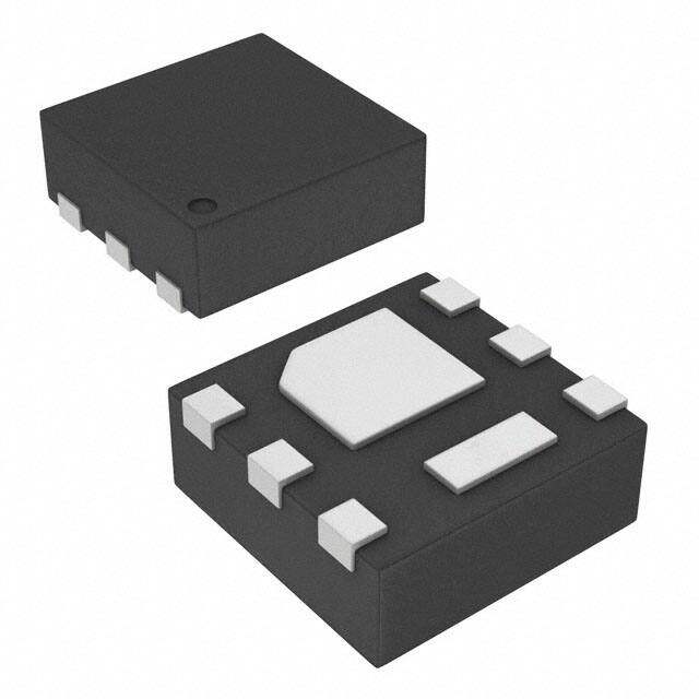
Package 6-WDFN Exposed Pad
Category Discrete Semiconductor Products / Transistors - FETs, MOSFETs - Single
Description
TEXAS INSTRUMENTS - CSD17313Q2 - MOSFET Transistor, N Channel, 5 A, 30 V, 0.024 ohm, 8 V, 1.3 V
PDF
/
Buying Options
Total Price: USD $0.41
Unit Price: USD $0.4136
≥1 USD $0.4136
≥10 USD $0.35552
≥100 USD $0.24728
≥500 USD $0.193054
≥1000 USD $0.156922
Inventory: 1626
Minimum: 1
-
+

Technical Details
Compliance
Lead Free Lead Free
RoHS Status ROHS3 Compliant
REACH SVHC No SVHC
Radiation Hardening No
Dimensions
Thickness 750μm
Width 2mm
Length 2mm
Height 800μm
Technical
Pulsed Drain Current-Max (IDM) 20A
Drain to Source Breakdown Voltage 30V
Drain-source On Resistance-Max 0.042Ohm
Drain Current-Max (Abs) (ID) 5A
Gate to Source Voltage (Vgs) 10V
Threshold Voltage 1.3V
Continuous Drain Current (ID) 5A
Turn-Off Delay Time 4.2 ns
Fall Time (Typ) 1.3 ns
Vgs (Max) +10V, -8V
Drive Voltage (Max Rds On,Min Rds On) 3V 8V
Rise Time 3.9 ns
Gate Charge (Qg) (Max) @ Vgs 2.7nC @ 4.5V
Current - Continuous Drain (Id) @ 25°C 5A Tc
Input Capacitance (Ciss) (Max) @ Vds 340pF @ 15V
Vgs(th) (Max) @ Id 1.8V @ 250μA
Rds On (Max) @ Id, Vgs 30m Ω @ 4A, 8V
Transistor Application SWITCHING
FET Type N-Channel
Turn On Delay Time 2.8 ns
Case Connection DRAIN
Power Dissipation 2.3W
Operating Mode ENHANCEMENT MODE
Element Configuration Single
Power Dissipation-Max 2.3W Ta
Number of Elements 1
Pin Count 8
Base Part Number CSD17313
Peak Reflow Temperature (Cel) 260
Terminal Position DUAL
Technology MOSFET (Metal Oxide)
Subcategory FET General Purpose Powers
Terminal Finish Nickel/Palladium/Gold (Ni/Pd/Au)
ECCN Code EAR99
Number of Terminations 6
Moisture Sensitivity Level (MSL) 1 (Unlimited)
Part Status Active
Pbfree Code yes
JESD-609 Code e4
Series NexFET?
Packaging Tape & Reel (TR)
Operating Temperature -55°C~150°C TJ
Physical
Transistor Element Material SILICON
Number of Pins 6
Package / Case 6-WDFN Exposed Pad
Mounting Type Surface Mount
Mount Surface Mount
Supply Chain
Lifecycle Status ACTIVE (Last Updated: 4 days ago)
Factory Lead Time 6 Weeks
Alternative Model

Recommended For You

CSD17313Q2+price,CSD17313Q2+datasheet,CSD17313Q2+in stock,buy+CSD17313Q2,finder+CSD17313Q2,CSD17313Q2+tutorials,CSD17313Q2+download