CSD16413Q5A
RoHS  RoHS compliant
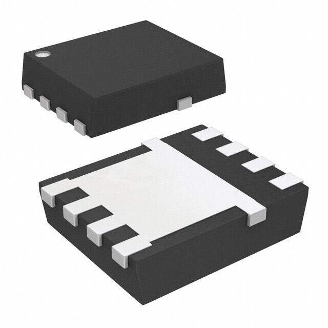
Package 8-PowerTDFN
Category Discrete Semiconductor Products / Transistors - FETs, MOSFETs - Single
Description
MOSFET N-CH 25V 100A 8-SON
PDF
/
Buying Options
Total Price: USD $0.64
Unit Price: USD $0.6365
≥1 USD $0.6365
≥10 USD $0.5225
≥100 USD $0.50635
≥500 USD $0.48925
≥1000 USD $0.4731
Inventory: 42805
Minimum: 1
-
+

Technical Details
Compliance
Lead Free Contains Lead
RoHS Status ROHS3 Compliant
REACH SVHC No SVHC
Radiation Hardening No
Dimensions
Thickness 1mm
Width 6mm
Length 4.9mm
Height 1.1mm
Technical
Nominal Vgs 1.6 V
Dual Supply Voltage 25V
Drain to Source Breakdown Voltage 25V
Drain-source On Resistance-Max 0.0056Ohm
Drain Current-Max (Abs) (ID) 24A
Gate to Source Voltage (Vgs) 16V
Threshold Voltage 1.6V
Continuous Drain Current (ID) 100A
Turn-Off Delay Time 10.7 ns
Fall Time (Typ) 5.7 ns
Vgs (Max) +16V, -12V
Drive Voltage (Max Rds On,Min Rds On) 4.5V 10V
Rise Time 15.9ns
Gate Charge (Qg) (Max) @ Vgs 11.7nC @ 4.5V
Current - Continuous Drain (Id) @ 25°C 24A Ta 100A Tc
Input Capacitance (Ciss) (Max) @ Vds 1780pF @ 12.5V
Vgs(th) (Max) @ Id 1.9V @ 250μA
Rds On (Max) @ Id, Vgs 3.9m Ω @ 24A, 10V
Transistor Application SWITCHING
FET Type N-Channel
Turn On Delay Time 9.1 ns
Case Connection DRAIN
Power Dissipation 3.1W
Operating Mode ENHANCEMENT MODE
Element Configuration Single
Power Dissipation-Max 3.1W Ta
Number of Elements 1
Pin Count 8
Base Part Number CSD16413
Peak Reflow Temperature (Cel) 260
Terminal Position DUAL
Technology MOSFET (Metal Oxide)
Subcategory FET General Purpose Power
Additional Feature AVALANCHE RATED
ECCN Code EAR99
Termination SMD/SMT
Number of Terminations 5
Moisture Sensitivity Level (MSL) 1 (Unlimited)
Part Status Active
Pbfree Code yes
JESD-609 Code e3
Series NexFET?
Packaging Cut Tape (CT)
Operating Temperature -55°C~150°C TJ
Physical
Transistor Element Material SILICON
Number of Pins 8
Package / Case 8-PowerTDFN
Mounting Type Surface Mount
Mount Surface Mount
Contact Plating Tin
Supply Chain
Lifecycle Status ACTIVE (Last Updated: 2 days ago)
Factory Lead Time 6 Weeks
Alternative Model

Recommended For You

CSD16413Q5A+price,CSD16413Q5A+datasheet,CSD16413Q5A+in stock,buy+CSD16413Q5A,finder+CSD16413Q5A,CSD16413Q5A+tutorials,CSD16413Q5A+download