STW60N65M5
RoHS  RoHS compliant
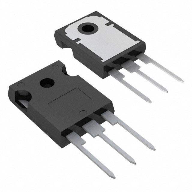
Package TO-247-3
Category Discrete Semiconductor Products / Transistors - FETs, MOSFETs - Single
Description
MOSFET N-Ch 650V 0.049 Ohm 46A Mdmesh V
PDF
/
Buying Options
Total Price: USD $10.1
Unit Price: USD $10.1024
≥1 USD $10.1024
≥10 USD $7.87453
≥100 USD $7.07557
≥500 USD $7.062
Inventory: 598
Minimum: 1
-
+

Technical Details
Compliance
RoHS Status ROHS3 Compliant
Lead Free Lead Free
REACH SVHC No SVHC
Radiation Hardening No
Dimensions
Width 5.15mm
Length 15.75mm
Height 20.15mm
Technical
Drain to Source Breakdown Voltage 650V
Gate to Source Voltage (Vgs) 25V
Threshold Voltage 4V
Continuous Drain Current (ID) 46A
Turn-Off Delay Time 13 ns
Fall Time (Typ) 16 ns
Vgs (Max) ±25V
Drive Voltage (Max Rds On,Min Rds On) 10V
Rise Time 11ns
Gate Charge (Qg) (Max) @ Vgs 139nC @ 10V
Current - Continuous Drain (Id) @ 25°C 46A Tc
Input Capacitance (Ciss) (Max) @ Vds 6810pF @ 100V
Vgs(th) (Max) @ Id 5V @ 250μA
Rds On (Max) @ Id, Vgs 59m Ω @ 23A, 10V
Transistor Application SWITCHING
FET Type N-Channel
Turn On Delay Time 90 ns
Power Dissipation 255W
Operating Mode ENHANCEMENT MODE
Element Configuration Single
Power Dissipation-Max 255W Tc
Number of Elements 1
Pin Count 3
Base Part Number STW60N
Technology MOSFET (Metal Oxide)
Subcategory FET General Purpose Power
Additional Feature ULTRA-LOW RESISTANCE
Terminal Finish Matte Tin (Sn)
Resistance 59MOhm
ECCN Code EAR99
Number of Terminations 3
Moisture Sensitivity Level (MSL) 1 (Unlimited)
Part Status Obsolete
Pbfree Code yes
JESD-609 Code e3
Series MDmesh? V
Packaging Tube
Operating Temperature 150°C TJ
Physical
Transistor Element Material SILICON
Number of Pins 3
Package / Case TO-247-3
Mounting Type Through Hole
Mount Through Hole
Alternative Model

Recommended For You

STW60N65M5+price,STW60N65M5+datasheet,STW60N65M5+in stock,buy+STW60N65M5,finder+STW60N65M5,STW60N65M5+tutorials,STW60N65M5+download