STW36N55M5
RoHS  RoHS compliant
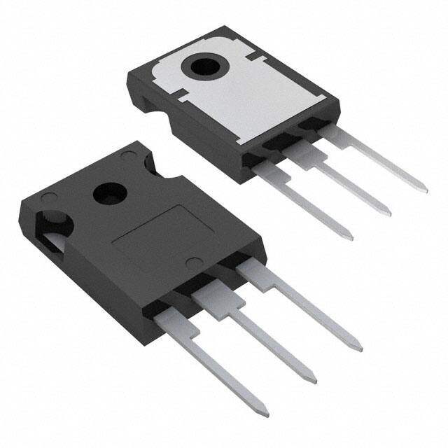
Package TO-247-3
Category Discrete Semiconductor Products / Transistors - FETs, MOSFETs - Single
Description
MOSFET N CH 550V 33A TO-247
PDF
/
Buying Options
Total Price: USD $0.68
Unit Price: USD $0.67857
≥1 USD $0.67857
≥10 USD $0.640166
≥100 USD $0.603927
≥500 USD $0.569742
≥1000 USD $0.537502
Inventory: 1133
Minimum: 1
-
+

Technical Details
Compliance
Lead Free Lead Free
RoHS Status ROHS3 Compliant
Radiation Hardening No
Dimensions
Width 5.15mm
Length 15.75mm
Height 20.15mm
Technical
Drain to Source Breakdown Voltage 550V
Drain-source On Resistance-Max 0.08Ohm
Gate to Source Voltage (Vgs) 25V
Continuous Drain Current (ID) 33A
Turn-Off Delay Time 56 ns
Vgs (Max) ±25V
Drive Voltage (Max Rds On,Min Rds On) 10V
Gate Charge (Qg) (Max) @ Vgs 62nC @ 10V
Current - Continuous Drain (Id) @ 25°C 33A Tc
Input Capacitance (Ciss) (Max) @ Vds 2950pF @ 100V
Vgs(th) (Max) @ Id 5V @ 250μA
Rds On (Max) @ Id, Vgs 80m Ω @ 16.5A, 10V
Transistor Application SWITCHING
FET Type N-Channel
Turn On Delay Time 56 ns
Power Dissipation 190W
Operating Mode ENHANCEMENT MODE
Element Configuration Single
Power Dissipation-Max 190W Tc
Number of Elements 1
Base Part Number STW36N
Technology MOSFET (Metal Oxide)
Subcategory FET General Purpose Power
ECCN Code EAR99
Number of Terminations 3
Moisture Sensitivity Level (MSL) 1 (Unlimited)
Part Status Active
Series MDmesh? V
Packaging Tube
Operating Temperature 150°C TJ
Physical
Transistor Element Material SILICON
Number of Pins 3
Package / Case TO-247-3
Mounting Type Through Hole
Mount Through Hole
Supply Chain
Factory Lead Time 17 Weeks
Alternative Model

Recommended For You

STW36N55M5+price,STW36N55M5+datasheet,STW36N55M5+in stock,buy+STW36N55M5,finder+STW36N55M5,STW36N55M5+tutorials,STW36N55M5+download