STV250N55F3
RoHS  RoHS compliant
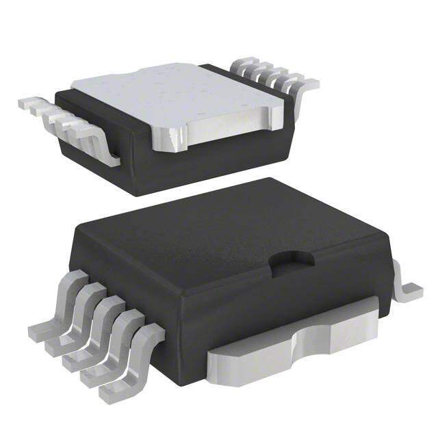
Package PowerSO-10 Exposed Bottom Pad
Category Discrete Semiconductor Products / Transistors - FETs, MOSFETs - Single
Description
MOSFET N-channel 55 V
PDF
/
Inventory: /
Minimum: /
The more specific your information, the faster response you will get.
Please complete the following form with the details of your request part and
contact information to get a quote.
Quotation Consultation
Technical Details
Compliance
Lead Free Lead Free
RoHS Status ROHS3 Compliant
Radiation Hardening No
Technical
Drain to Source Breakdown Voltage 55V
Drain Current-Max (Abs) (ID) 250A
Gate to Source Voltage (Vgs) 20V
Continuous Drain Current (ID) 200A
Turn-Off Delay Time 110 ns
Fall Time (Typ) 50 ns
Vgs (Max) ±20V
Drive Voltage (Max Rds On,Min Rds On) 10V
Rise Time 150ns
Gate Charge (Qg) (Max) @ Vgs 100nC @ 10V
Current - Continuous Drain (Id) @ 25°C 200A Tc
Input Capacitance (Ciss) (Max) @ Vds 6800pF @ 25V
Vgs(th) (Max) @ Id 4V @ 250μA
Rds On (Max) @ Id, Vgs 2.2m Ω @ 75A, 10V
Transistor Application SWITCHING
FET Type N-Channel
Turn On Delay Time 25 ns
Case Connection DRAIN
Power Dissipation 300W
Operating Mode ENHANCEMENT MODE
Element Configuration Single
Power Dissipation-Max 300W Tc
Number of Elements 1
Pin Count 10
Base Part Number STV250
Peak Reflow Temperature (Cel) 250
Terminal Form GULL WING
Terminal Position DUAL
Technology MOSFET (Metal Oxide)
Subcategory FET General Purpose Power
Terminal Finish Matte Tin (Sn) - annealed
Resistance 2.2MOhm
ECCN Code EAR99
Number of Terminations 10
Moisture Sensitivity Level (MSL) 1 (Unlimited)
Part Status Obsolete
Pbfree Code yes
JESD-609 Code e3
Series STripFET? III
Packaging Tape & Reel (TR)
Operating Temperature -55°C~175°C TJ
Physical
Transistor Element Material SILICON
Number of Pins 10
Package / Case PowerSO-10 Exposed Bottom Pad
Mounting Type Surface Mount
Mount Surface Mount
Alternative Model

Recommended For You

STV250N55F3+price,STV250N55F3+datasheet,STV250N55F3+in stock,buy+STV250N55F3,finder+STV250N55F3,STV250N55F3+tutorials,STV250N55F3+download