STP15NK50ZFP
RoHS  RoHS compliant
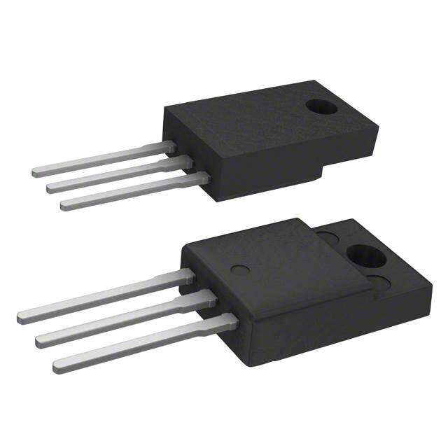
Package TO-220-3 Full Pack
Category Discrete Semiconductor Products / Transistors - FETs, MOSFETs - Single
Description
MOSFET N Ch 500V Zener SuperMESH
PDF
/
Buying Options
Total Price: USD $2.28
Unit Price: USD $2.28285
≥1 USD $2.28285
≥10 USD $1.87245
≥100 USD $1.8145
≥500 USD $1.7556
≥1000 USD $1.69765
Inventory: 428
Minimum: 1
-
+

Technical Details
Compliance
Lead Free Lead Free
RoHS Status ROHS3 Compliant
REACH SVHC No SVHC
Dimensions
Width 4.6mm
Length 10.4mm
Height 9.3mm
Technical
Pulsed Drain Current-Max (IDM) 56A
Drain to Source Breakdown Voltage 500V
Gate to Source Voltage (Vgs) 30V
JEDEC-95 Code TO-220AB
Threshold Voltage 3.75V
Continuous Drain Current (ID) 14A
Turn-Off Delay Time 62 ns
Fall Time (Typ) 15 ns
Vgs (Max) ±30V
Drive Voltage (Max Rds On,Min Rds On) 10V
Rise Time 23 ns
Gate Charge (Qg) (Max) @ Vgs 106nC @ 10V
Current - Continuous Drain (Id) @ 25°C 14A Tc
Input Capacitance (Ciss) (Max) @ Vds 2260pF @ 25V
Vgs(th) (Max) @ Id 4.5V @ 100μA
Rds On (Max) @ Id, Vgs 340m Ω @ 7A, 10V
Transistor Application SWITCHING
FET Type N-Channel
Turn On Delay Time 20 ns
Case Connection ISOLATED
Power Dissipation 40W
Operating Mode ENHANCEMENT MODE
Element Configuration Single
Power Dissipation-Max 40W Tc
Number of Elements 1
Qualification Status Not Qualified
Pin Count 3
Base Part Number STP15N
Time@Peak Reflow Temperature-Max (s) NOT SPECIFIED
Current Rating 14A
Reach Compliance Code not_compliant
Peak Reflow Temperature (Cel) NOT SPECIFIED
Technology MOSFET (Metal Oxide)
Voltage - Rated DC 500V
Subcategory FET General Purpose Power
Additional Feature HIGH VOLTAGE
Terminal Finish Matte Tin (Sn) - annealed
ECCN Code EAR99
Number of Terminations 3
Moisture Sensitivity Level (MSL) 1 (Unlimited)
Part Status Active
JESD-609 Code e3
Series SuperMESH?
Packaging Tube
Operating Temperature -50°C~150°C TJ
Physical
Transistor Element Material SILICON
Weight 9.071847g
Number of Pins 3
Package / Case TO-220-3 Full Pack
Mounting Type Through Hole
Mount Through Hole
Supply Chain
Lifecycle Status ACTIVE (Last Updated: 7 months ago)
Factory Lead Time 12 Weeks
Alternative Model

Recommended For You

STP15NK50ZFP+price,STP15NK50ZFP+datasheet,STP15NK50ZFP+in stock,buy+STP15NK50ZFP,finder+STP15NK50ZFP,STP15NK50ZFP+tutorials,STP15NK50ZFP+download