STN3P6F6
RoHS  RoHS compliant
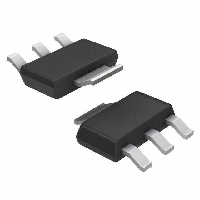
Package TO-261-4, TO-261AA
Category Discrete Semiconductor Products / Transistors - FETs, MOSFETs - Single
Description
MOSFET P-CH 60V SOT-223
PDF
/
Buying Options
Total Price: USD $0.81
Unit Price: USD $0.8096
≥1 USD $0.8096
≥10 USD $0.66352
≥100 USD $0.51612
≥500 USD $0.437448
≥1000 USD $0.356338
≥3000 USD $0.335456
Inventory: 10312
Minimum: 1
-
+

Technical Details
Compliance
Lead Free Lead Free
RoHS Status ROHS3 Compliant
REACH SVHC No SVHC
Dimensions
Width 3.7mm
Length 6.7mm
Height 1.9mm
Technical
Max Junction Temperature (Tj) 175°C
Drain to Source Breakdown Voltage -60V
Drain Current-Max (Abs) (ID) 3A
Gate to Source Voltage (Vgs) 20V
Threshold Voltage -4V
Continuous Drain Current (ID) -3A
Turn-Off Delay Time 14 ns
Fall Time (Typ) 3.7 ns
Vgs (Max) ±20V
Drive Voltage (Max Rds On,Min Rds On) 10V
Drain to Source Voltage (Vdss) 60V
Rise Time 5.3 ns
Gate Charge (Qg) (Max) @ Vgs 6.4nC @ 10V
Input Capacitance (Ciss) (Max) @ Vds 340pF @ 48V
Vgs(th) (Max) @ Id 4V @ 250μA
Rds On (Max) @ Id, Vgs 160m Ω @ 1.5A, 10V
Transistor Application SWITCHING
FET Type P-Channel
Turn On Delay Time 6.4 ns
Case Connection DRAIN
Power Dissipation 2.6W
Operating Mode ENHANCEMENT MODE
Element Configuration Single
Power Dissipation-Max 2.6W Tc
Number of Channels 1
Number of Elements 1
Base Part Number STN3P
Reach Compliance Code not_compliant
Terminal Form GULL WING
Terminal Position DUAL
Technology MOSFET (Metal Oxide)
Terminal Finish Matte Tin (Sn)
Resistance 130MOhm
ECCN Code EAR99
Number of Terminations 4
Moisture Sensitivity Level (MSL) 1 (Unlimited)
Part Status Active
JESD-609 Code e3
Series DeepGATE?, STripFET? VI
Packaging Cut Tape (CT)
Operating Temperature -55°C~175°C TJ
Physical
Transistor Element Material SILICON
Number of Pins 4
Package / Case TO-261-4, TO-261AA
Mounting Type Surface Mount
Mount Surface Mount
Supply Chain
Lifecycle Status ACTIVE (Last Updated: 8 months ago)
Factory Lead Time 20 Weeks
Alternative Model

Recommended For You

STN3P6F6+price,STN3P6F6+datasheet,STN3P6F6+in stock,buy+STN3P6F6,finder+STN3P6F6,STN3P6F6+tutorials,STN3P6F6+download